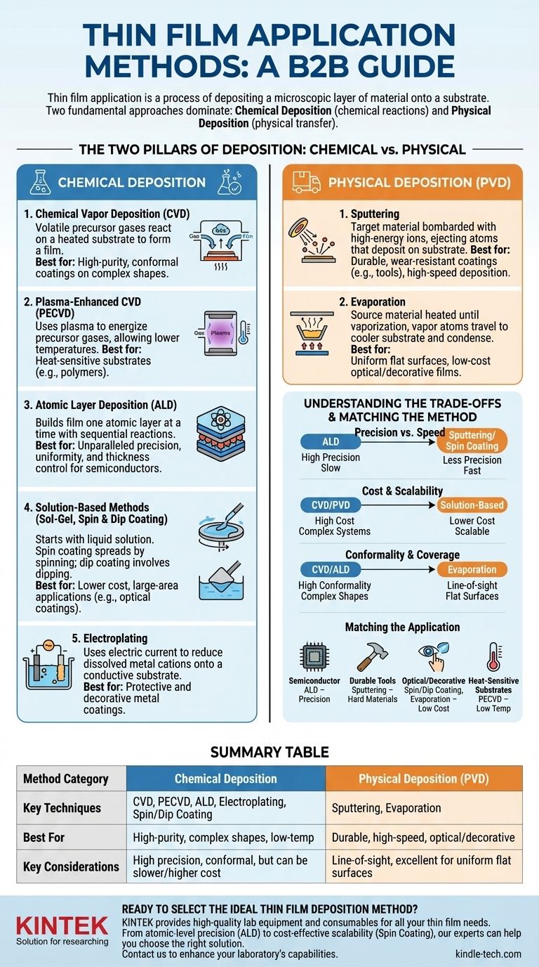
At its core, thin film application is a process of depositing a microscopic layer of material onto a substrate. These methods are broadly categorized into two fundamental approaches: Chemical Deposition, which uses chemical reactions to form the film, and Physical Deposition, which physically transfers material from a source to the substrate.
The choice of a thin film deposition method is not arbitrary. It is a critical engineering decision dictated by the required film properties—such as precision, purity, and uniformity—and the practical constraints of the final application, including cost and scale.
The Two Pillars of Deposition: Chemical vs. Physical
Understanding the fundamental difference between chemical and physical deposition is the first step in navigating this field. One creates the material directly on the surface, while the other moves existing material onto it.
Understanding Chemical Deposition
Chemical deposition methods use precursor materials, often in a gas or liquid state, that undergo a chemical reaction on the substrate's surface, leaving a solid film behind.
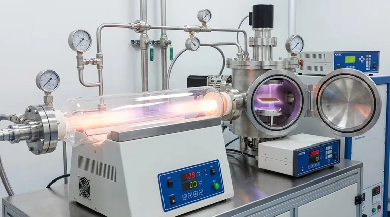
Chemical Vapor Deposition (CVD) In CVD, volatile precursor gases are introduced into a reaction chamber where they decompose and react on a heated substrate to form the desired film. It's known for creating high-purity, conformal coatings on complex shapes.
Plasma-Enhanced CVD (PECVD) This is a variation of CVD that uses a plasma to energize the precursor gases. This allows deposition to occur at much lower temperatures, making it suitable for substrates that cannot withstand high heat.
Atomic Layer Deposition (ALD) ALD is a highly precise technique that builds a film one atomic layer at a time. It involves sequential, self-limiting chemical reactions, offering unparalleled control over film thickness and uniformity, which is critical for modern semiconductor manufacturing.
Solution-Based Methods (Sol-Gel, Spin & Dip Coating) These methods start with a liquid chemical solution (a "sol"). In spin coating, the substrate is spun at high speed to spread the liquid into a uniform film. In dip coating, the substrate is simply dipped into and withdrawn from the solution. These techniques are often lower-cost and simpler to implement.
Electroplating This classic method uses an electric current to reduce dissolved metal cations so that they form a thin, coherent metal coating on an electrode. It is widely used for both protective and decorative applications.
Understanding Physical Deposition
Physical deposition methods, often categorized as Physical Vapor Deposition (PVD), involve mechanically or thermally transporting material from a source "target" to the substrate, typically within a vacuum environment.
Sputtering In sputtering, a target of the desired material is bombarded with high-energy ions from a plasma. This collision ejects or "sputters" atoms from the target, which then travel and deposit onto the substrate, forming the thin film.
Evaporation This method involves heating the source material in a high-vacuum chamber until it vaporizes. These vaporized atoms then travel in a straight line to the cooler substrate, where they condense back into a solid state, creating the film.
Understanding the Trade-offs
No single deposition method is universally superior. The optimal choice depends entirely on a balance of technical requirements and economic realities.
Precision vs. Speed
There is often a direct trade-off between the precision of the film and the speed of the process. ALD offers atomic-level control but is inherently slow. In contrast, methods like sputtering or spin coating are significantly faster but offer less fine-grained control over thickness.
Cost and Scalability
High-vacuum systems required for CVD and PVD are a significant capital expense. Solution-based methods like dip coating are generally far less expensive and can be easier to scale for large-area applications, like architectural glass.
Conformality and Coverage
The ability to uniformly coat complex, three-dimensional shapes is known as conformality. CVD and ALD excel at this because the precursor gases can reach every nook and cranny. Line-of-sight physical methods like evaporation struggle with complex geometries.
Matching the Method to Your Application
Your end goal is the single most important factor in selecting a deposition technique.
- If your primary focus is ultimate precision for semiconductor devices: ALD is the industry standard for creating the incredibly thin, uniform layers required for modern transistors.
- If your primary focus is a durable, wear-resistant coating for tools: PVD methods like sputtering are ideal for depositing hard materials like titanium nitride.
- If your primary focus is a low-cost optical or decorative coating: Spin coating, dip coating, or evaporation are highly effective and economical choices for applications like anti-reflective lens coatings or jewelry.
- If your primary focus is coating a heat-sensitive substrate like a polymer: PECVD is the superior choice, as its low-temperature process prevents damage to the underlying material.
Ultimately, understanding these methods and their trade-offs empowers you to intentionally design materials with the exact properties your project demands.
Summary Table:
| Method Category | Key Techniques | Best For | Key Considerations |
|---|---|---|---|
| Chemical Deposition | CVD, PECVD, ALD, Electroplating, Spin/Dip Coating | High-purity films, complex shapes, low-temperature processes | High precision, conformal coatings, but can be slower/higher cost |
| Physical Deposition (PVD) | Sputtering, Evaporation | Durable coatings, high-speed deposition, optical/decorative films | Line-of-sight limitation, excellent for uniform flat surfaces |
Ready to select the ideal thin film deposition method for your application? At KINTEK, we specialize in providing high-quality lab equipment and consumables for all your thin film needs. Whether you require the atomic-level precision of ALD for semiconductor research or the cost-effective scalability of spin coating for large-area projects, our experts can help you choose the right solution. Contact us today to discuss your specific requirements and discover how KINTEK can enhance your laboratory's capabilities and efficiency.
Visual Guide
Related Products
- Aluminized Ceramic Evaporation Boat for Thin Film Deposition
- Tungsten Evaporation Boat for Thin Film Deposition
- Electron Beam Evaporation Coating Oxygen-Free Copper Crucible and Evaporation Boat
- Molybdenum Tungsten Tantalum Evaporation Boat for High Temperature Applications
- HFCVD Machine System Equipment for Drawing Die Nano-Diamond Coating
People Also Ask
- What is the widely used boat made of in thermal evaporation? Choosing the Right Material for High-Purity Deposition
- What is the chemical method for thin film deposition? Build Films from the Molecular Level Up
- What are thin films deposited by evaporation? A Guide to High-Purity Coating
- Why is an alumina boat selected for catalyst precursors? Ensure Sample Purity at 1000 °C
- What is the source of evaporation for thin film? Choosing Between Thermal and E-Beam Methods


