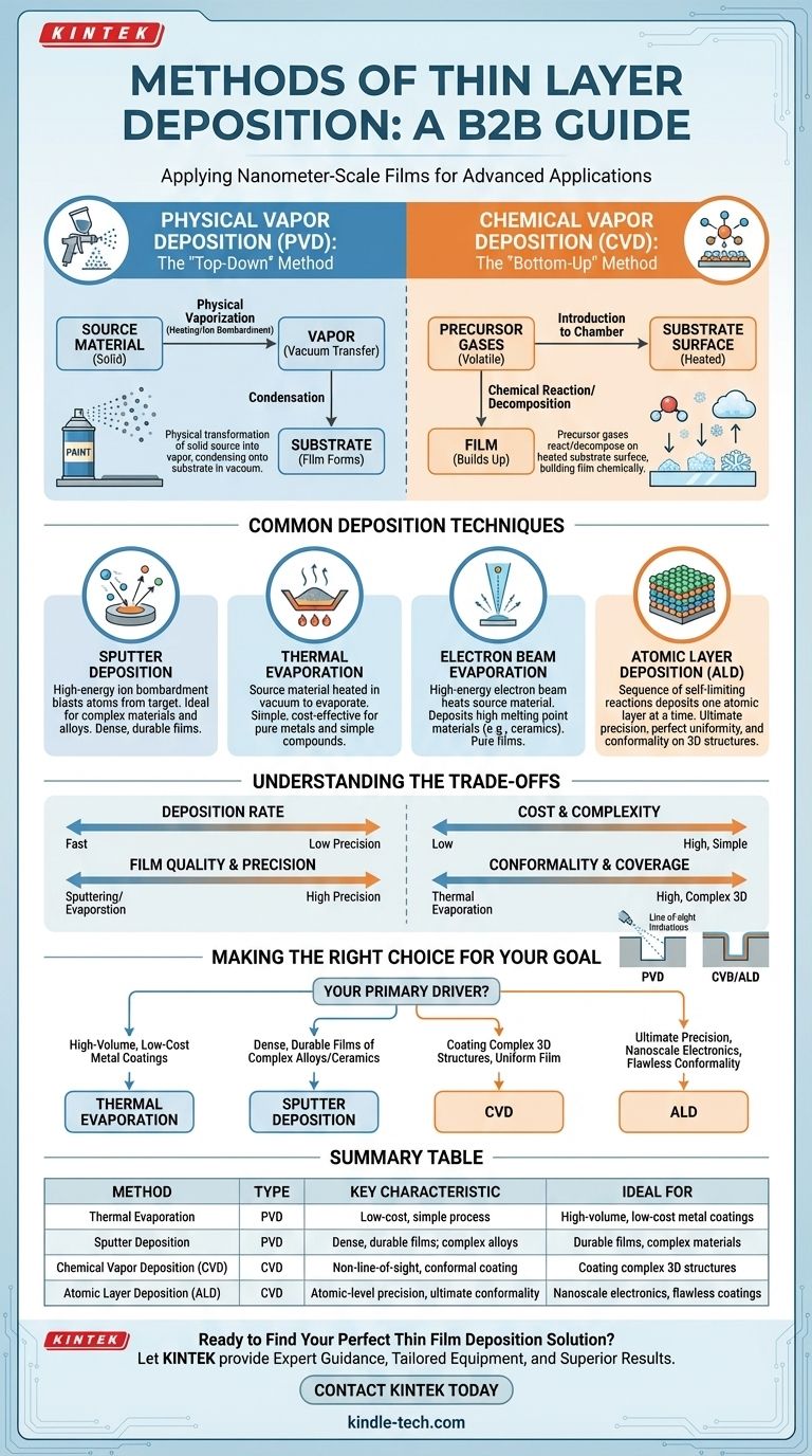
At its core, thin layer deposition is the process of applying a film of material, often only nanometers or micrometers thick, onto a substrate. The primary methods fall into two major categories: Physical Vapor Deposition (PVD), where a material is physically vaporized and transferred, and Chemical Vapor Deposition (CVD), where chemical reactions on the substrate surface form the film. More advanced techniques like Atomic Layer Deposition (ALD) offer layer-by-layer precision, while methods like Spray Pyrolysis are used for specific applications.
Choosing the right deposition method is not about finding the single "best" technique. It is about matching the process—whether physical or chemical—to your specific material, desired film properties, and operational constraints like cost and scale.
The Two Fundamental Approaches: Physical vs. Chemical
The vast landscape of deposition techniques can be simplified by understanding the core difference between physically moving material and chemically creating it.
Physical Vapor Deposition (PVD): The "Top-Down" Method
PVD encompasses a family of processes that use physical means, like heating or ion bombardment, to transform a solid source material into a vapor. This vapor then travels through a vacuum and condenses onto the substrate, forming the thin film.
Think of PVD as a highly controlled form of spray painting. You have a source of "paint" (the material) that is atomized and directed at the target surface (the substrate).
Chemical Vapor Deposition (CVD): The "Bottom-Up" Method
CVD uses volatile precursor gases that are introduced into a reaction chamber. These gases react or decompose on the heated substrate surface, "building" the thin film from the bottom up.
The process is analogous to frost forming on a cold window. Water vapor molecules in the air (the precursors) settle on the cold glass (the substrate) and assemble into a solid, crystalline layer of ice (the film).
A Closer Look at Common Deposition Techniques
While PVD and CVD are the main families, the specific techniques within them offer distinct advantages.
Sputter Deposition (PVD)
In sputtering, a target made of the desired material is bombarded by high-energy ions from a plasma. This bombardment acts like a microscopic sandblaster, knocking atoms off the target, which then travel and deposit onto the substrate.
This method is extremely versatile and excellent for depositing complex materials like alloys and compounds, as the composition of the film closely matches the source target.
Thermal Evaporation (PVD)
This is one of the simplest PVD methods. The source material is placed in a container (like a crucible or boat) and heated in a vacuum until it evaporates. The resulting vapor rises, travels in a straight line, and condenses on the cooler substrate.
It is a cost-effective choice for depositing pure metals and simple compounds with relatively low melting points.
Electron Beam Evaporation (PVD)
A variation of thermal evaporation, e-beam evaporation uses a high-energy, magnetically focused electron beam to heat the source material. This allows for the deposition of materials with very high melting points, such as refractory metals and ceramics, which are difficult to evaporate thermally.
Because only the material itself is heated, it results in purer films with less contamination from the heating source.
Atomic Layer Deposition (ALD)
ALD is a subtype of CVD that offers the ultimate level of precision. The process uses a sequence of self-limiting chemical reactions, depositing the film literally one atomic layer at a time.
This technique provides unparalleled control over film thickness and can create perfectly uniform, pinhole-free coatings on even the most complex 3D structures.
Understanding the Trade-offs
No single method is universally superior. The optimal choice depends entirely on your specific requirements for performance, material, and cost.
Cost vs. Precision
Simpler methods like thermal evaporation are generally the least expensive. Sputtering systems are more complex and costly, while ALD systems represent a significant investment due to their precision and slower processing time.
Material Compatibility
Thermal evaporation can cause some complex alloys or compounds to decompose if their components have different vapor pressures. Sputtering is far more robust for maintaining the stoichiometry of complex materials. CVD and ALD depend entirely on the availability of suitable, often highly reactive, precursor gases.
Conformality and Coverage
Conformality is the ability of a film to uniformly coat a non-flat surface. PVD techniques are "line-of-sight" processes, making it difficult to coat complex shapes, trenches, or the backside of a substrate. In contrast, CVD and ALD excel at creating highly conformal coatings because the precursor gases can reach all exposed surfaces.
Deposition Rate vs. Film Quality
There is often a trade-off between speed and control. Sputtering and evaporation offer relatively high deposition rates suitable for production. ALD is significantly slower, building the film angstrom by angstrom, but this slow pace is what guarantees its exceptional quality and precision.
Making the Right Choice for Your Goal
Your application's primary driver should guide your decision.
- If your primary focus is high-volume, low-cost coatings of simple metals: Thermal evaporation is often the most economical and straightforward choice.
- If your primary focus is depositing dense, durable films of complex alloys or ceramics: Sputter deposition offers superior control over composition and film properties.
- If your primary focus is coating complex 3D structures with a perfectly uniform film: CVD's non-line-of-sight nature makes it the ideal choice.
- If your primary focus is ultimate precision, atomic-level thickness control, and flawless conformality for nanoscale electronics or optics: ALD is the unmatched, albeit slower and more expensive, solution.
Understanding these fundamental trade-offs transforms the choice of a deposition method from a guess into a strategic engineering decision.
Summary Table:
| Method | Type | Key Characteristic | Ideal For |
|---|---|---|---|
| Thermal Evaporation | PVD | Low-cost, simple process | High-volume, low-cost metal coatings |
| Sputter Deposition | PVD | Dense, durable films; complex alloys | Durable films, complex materials |
| Chemical Vapor Deposition (CVD) | CVD | Non-line-of-sight, conformal coating | Coating complex 3D structures |
| Atomic Layer Deposition (ALD) | CVD | Atomic-level precision, ultimate conformality | Nanoscale electronics, flawless coatings |
Ready to Find Your Perfect Thin Film Deposition Solution?
Choosing the right deposition method is critical for your project's success. The experts at KINTEK specialize in lab equipment and consumables for all your thin film needs. We can help you select the ideal PVD, CVD, or ALD system to match your specific materials, desired film properties, and budget.
Let KINTEK provide the solution for your laboratory:
- Expert Guidance: Navigate the trade-offs between cost, precision, and material compatibility.
- Tailored Equipment: Find the perfect system for sputtering, evaporation, CVD, or ALD processes.
- Superior Results: Achieve the precise, high-quality thin films your research or production demands.
Contact our team today for a personalized consultation!
Visual Guide
Related Products
- Tungsten Evaporation Boat for Thin Film Deposition
- Aluminized Ceramic Evaporation Boat for Thin Film Deposition
- Thin-Layer Spectral Electrolysis Electrochemical Cell
- Electron Beam Evaporation Coating Oxygen-Free Copper Crucible and Evaporation Boat
- Molybdenum Tungsten Tantalum Evaporation Boat for High Temperature Applications
People Also Ask
- What is a thin film evaporator? A Gentle Solution for Heat-Sensitive & Viscous Materials
- What is the process of thin film deposition? A Guide to PVD, CVD, and Coating Techniques
- What are the two primary categories of deposition technologies? PVD vs. CVD Explained
- What is the source of evaporation for thin film? Choosing Between Thermal and E-Beam Methods
- What methods are used to deposit thin films? A Guide to PVD, CVD, and ALD Techniques


