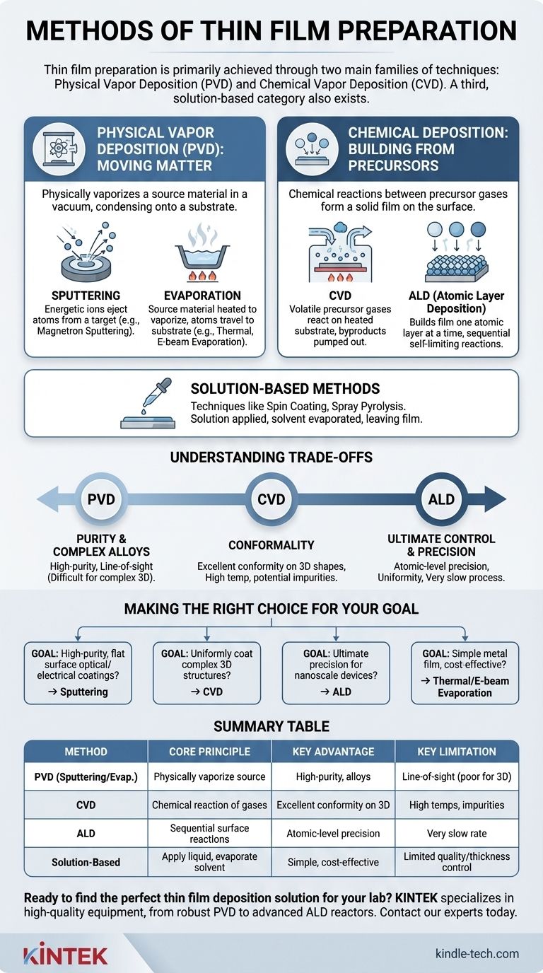
At the highest level, thin film preparation is achieved through two main families of techniques: Physical Vapor Deposition (PVD) and Chemical Vapor Deposition (CVD). PVD involves physically vaporizing a source material in a vacuum and allowing it to condense onto a substrate, while CVD uses chemical reactions between precursor gases to form a solid film directly on the substrate's surface. A third category of solution-based methods, like spin coating, also exists for specific applications.
The critical distinction between thin film methods is fundamental: Physical techniques move existing material onto a surface, while chemical techniques build new material at the surface. Your choice depends entirely on the required film purity, conformity, temperature tolerance, and production scale.
The Pillars of Deposition: Physical vs. Chemical
The vast number of deposition techniques can be understood by separating them into two core strategies. This primary classification dictates the equipment, process conditions, and the resulting properties of the film.
Physical Vapor Deposition (PVD): Moving Matter
PVD encompasses a family of processes where a solid or liquid source material is converted into a vapor and transported to the substrate through a low-pressure, vacuum environment.
Key PVD Method: Sputtering
Sputtering involves bombarding a source material, known as the target, with energetic ions (usually an inert gas like argon). This collision physically ejects or "sputters" atoms from the target, which then travel and deposit onto the substrate. Magnetron sputtering is a common enhancement that uses magnetic fields to increase efficiency.
Key PVD Method: Evaporation
This is a more intuitive PVD process where the source material is heated in a vacuum chamber until it vaporizes. These vaporized atoms travel in a straight line until they condense on the cooler substrate, forming the thin film. Methods like thermal evaporation and e-beam evaporation are common variants.
Chemical Deposition: Building from Precursors
Instead of physically moving a source material, chemical deposition methods introduce precursor chemicals (usually as a gas or liquid) that react to form the desired solid film on the substrate surface.
Chemical Vapor Deposition (CVD)
In a CVD process, one or more volatile precursor gases are introduced into a reaction chamber. When these gases come into contact with a heated substrate, they react or decompose, leaving behind a solid film. The byproducts of the reaction are then pumped out of the chamber.
Atomic Layer Deposition (ALD)
ALD is a specialized subset of CVD that offers unparalleled precision. It builds the film one atomic layer at a time by introducing precursor gases sequentially. Each step is a self-limiting reaction, which provides exceptional control over thickness and uniformity, even on complex 3D structures.
Solution-Based Methods
Techniques like spin coating or spray pyrolysis are fundamentally different as they do not typically require a vacuum. A solution containing the desired material is applied to a substrate, and the solvent is then evaporated (often with heat), leaving the thin film behind.
Understanding the Trade-offs
No single deposition method is universally superior. The optimal choice is always a matter of balancing competing requirements for performance, cost, and material compatibility.
PVD: Purity vs. Line-of-Sight
The primary advantage of PVD is the ability to deposit high-purity films and complex alloys. However, because the vaporized atoms travel in straight lines, PVD is a line-of-sight technique. This makes it difficult to uniformly coat complex, non-planar shapes.
CVD: Conformality vs. Complexity
CVD's greatest strength is its ability to create highly conformal coatings that uniformly cover intricate 3D geometries. The trade-offs are that it often requires high substrate temperatures and the chemical reactions can introduce impurities into the film.
ALD: Ultimate Control vs. Speed
ALD provides the ultimate level of control, enabling the creation of perfectly uniform and pinhole-free films with atomic-level precision. This precision comes at the cost of speed; ALD is an extremely slow process, making it impractical for depositing thick films.
Making the Right Choice for Your Goal
Selecting the right method requires matching the technique's strengths to your project's primary objective.
- If your primary focus is high-purity optical or electrical coatings on flat surfaces: Sputtering offers excellent film density and control over material properties for applications like glass and electronics.
- If your primary focus is uniformly coating complex 3D structures: CVD is the superior choice due to its non-line-of-sight nature, essential for many semiconductor applications.
- If your primary focus is ultimate precision for nanoscale devices: ALD provides the atomic-level control required for modern transistors and advanced electronics, despite being slow.
- If your primary focus is depositing a simple metal film cost-effectively: Thermal or e-beam evaporation is often a highly efficient solution for applications like OLEDs or solar panels.
Understanding these fundamental principles empowers you to select the deposition technique that aligns perfectly with your material, structure, and performance targets.
Summary Table:
| Method | Core Principle | Key Advantage | Key Limitation |
|---|---|---|---|
| PVD (Sputtering/Evaporation) | Physically vaporize source material in a vacuum | High-purity films, good for alloys | Line-of-sight (poor for complex 3D shapes) |
| CVD | Chemical reaction of precursor gases on a heated substrate | Excellent conformity on complex 3D structures | Often requires high temperatures, potential impurities |
| ALD | Sequential, self-limiting surface reactions | Atomic-level precision and uniformity | Very slow deposition rate |
| Solution-Based (e.g., Spin Coating) | Apply a liquid precursor and evaporate the solvent | Simple, cost-effective, no vacuum needed | Limited film quality and thickness control |
Ready to find the perfect thin film deposition solution for your lab? The right equipment is critical for achieving the purity, conformity, and precision your research demands. At KINTEK, we specialize in providing high-quality lab equipment and consumables for all your deposition needs, from robust PVD systems to advanced ALD reactors. Our experts can help you select the ideal technology for your specific application, whether you're working on semiconductors, optics, or advanced materials. Contact our team today to discuss your project and discover how KINTEK can enhance your laboratory's capabilities.
Visual Guide
Related Products
- Aluminized Ceramic Evaporation Boat for Thin Film Deposition
- Tungsten Evaporation Boat for Thin Film Deposition
- Electron Beam Evaporation Coating Oxygen-Free Copper Crucible and Evaporation Boat
- Molybdenum Tungsten Tantalum Evaporation Boat for High Temperature Applications
- HFCVD Machine System Equipment for Drawing Die Nano-Diamond Coating
People Also Ask
- What is thin film deposition? Unlock Advanced Surface Engineering for Your Materials
- What is the chemical method for thin film deposition? Build Films from the Molecular Level Up
- What are the applications of thin films deposition? Unlock New Possibilities for Your Materials
- Why is an alumina boat and Ti3AlC2 powder bed necessary for Ti2AlC sintering? Protect MAX Phase Purity
- What is the widely used boat made of in thermal evaporation? Choosing the Right Material for High-Purity Deposition


