At its core, a thin film is an engineered layer of material, ranging from a single layer of atoms to several micrometers thick, that is intentionally deposited onto a surface, known as a substrate. The principles governing a thin film are not just about the material itself, but about the profound ways its properties change due to its extreme thinness, its interaction with the substrate, and the precise method used to create it.
The function and performance of a thin film are an emergent property. They arise from the critical interplay between the film's material composition, its precise thickness, the nature of its underlying substrate, and the deposition technique used to apply it.
The Foundational Principles of Thin Film Behavior
To understand thin films is to understand that they are not standalone materials. They are a component of a larger system, where each element influences the final outcome.
Principle 1: The Substrate as a Foundation
A thin film is never created in isolation; it is always deposited on a substrate, such as glass, silicon, or metal. The substrate is an active part of the system.
Its properties—like thermal expansion, surface roughness, and chemical composition—directly influence the adhesion, internal stress, and structural integrity of the film grown on top of it. A mismatch can lead to cracking, peeling, or a complete failure of the film's intended function.
Principle 2: Thickness Defines Function
The most defining characteristic of a thin film is its thickness, which is suppressed to a microscopic or nanoscopic scale. This dimensional constraint is what gives rise to many of its unique properties.
For example, a film's optical properties, such as its color or reflectivity, can be precisely tuned by controlling its thickness down to the nanometer. Similarly, its electrical conductivity and mechanical durability are functions of its thickness. A change of just a few nanometers can completely alter the film's performance.
Principle 3: Deposition Method Is Destiny
How a thin film is made is just as important as what it is made of. The deposition process controls the film's microstructure, density, purity, and uniformity, which in turn dictate its final properties.
These fabrication techniques fall into broad categories, each imparting different characteristics to the film. The choice of method is a fundamental engineering decision based on the desired outcome.
How Thin Films Are Created: Key Deposition Techniques
The deposition method directly engineers the film's properties at the atomic level. The two most common families of techniques are Chemical Vapor Deposition and Physical Vapor Deposition.
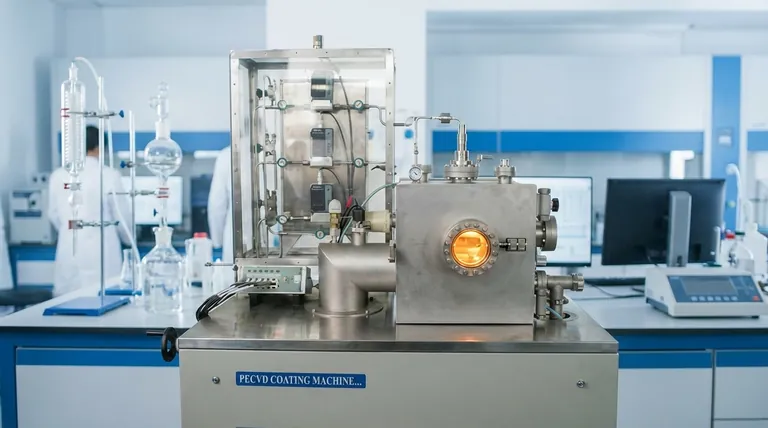
Chemical Vapor Deposition (CVD)
In CVD, the substrate is exposed to one or more volatile precursor gases. These gases react or decompose on the substrate's surface, leaving behind a high-quality, solid material layer.
This method is prized for its ability to create highly uniform and pure films that conform perfectly to complex surface shapes, making it essential for the semiconductor industry.
Physical Vapor Deposition (PVD)
PVD describes a set of vacuum deposition methods where a material is physically transferred from a source to a substrate. This is often done through evaporation (heating the material until it vaporizes) or sputtering (bombarding the material with high-energy ions, which ejects atoms that then land on the substrate).
PVD is a highly versatile process used to create everything from reflective coatings on mirrors to hard, wear-resistant coatings on machine tools.
Other Modifying Processes
Once a film is deposited, its properties can be further tuned. Processes like ion implantation can modify surface chemistry, while vacuum annealing (thermal processing) can alter the film's crystal structure and reduce internal stress.
Understanding the Trade-offs
Engineering a thin film is a process of balancing competing factors. There is no single "best" method, only the most appropriate one for a specific application.
The Substrate-Film Mismatch
A primary challenge is ensuring compatibility between the film and the substrate. A significant mismatch in thermal expansion coefficients can cause the film to crack or delaminate when the temperature changes. Poor chemical bonding can also lead to adhesion failure.
Deposition Complexity vs. Film Quality
Achieving a perfectly uniform, dense, and pure film often requires sophisticated and expensive equipment operating in a high vacuum. Simpler, faster deposition methods may be cheaper, but they often sacrifice control over the film's final microstructure and performance.
The Durability Challenge
By their nature, thin films can be mechanically fragile. Characteristics like scratch resistance and long-term durability are not inherent; they must be specifically designed for by choosing the right material and deposition process to ensure a dense, well-adhered layer.
Making the Right Choice for Your Goal
The optimal approach to designing a thin film is dictated entirely by its intended function. By understanding the core principles, you can prioritize the right variables.
- If your primary focus is optical performance (e.g., anti-reflection coatings): Precise control over film thickness is the most critical factor to manage light wave interference.
- If your primary focus is electronic applications (e.g., semiconductors): Material purity and structural uniformity are paramount, making CVD in a controlled vacuum environment the preferred method.
- If your primary focus is mechanical properties (e.g., wear-resistant coatings): Film density and strong adhesion to the substrate are key, putting focus on surface preparation and energetic deposition methods like sputtering.
Understanding these core principles allows you to move beyond viewing thin films as simple coatings and start leveraging them as precisely engineered materials.
Summary Table:
| Principle | Key Factor | Impact on Film |
|---|---|---|
| Foundation | Substrate Material | Determines adhesion, stress, and structural integrity. |
| Function | Film Thickness | Defines optical, electrical, and mechanical properties. |
| Fabrication | Deposition Method (CVD/PVD) | Controls microstructure, purity, and uniformity. |
Ready to Engineer Your Next Thin Film Solution?
Understanding these principles is the first step. Applying them to achieve a specific optical, electronic, or mechanical property requires the right equipment and expertise.
KINTEK specializes in precision lab equipment and consumables for thin film deposition and analysis. Whether you are developing semiconductors, optical coatings, or wear-resistant surfaces, we provide the reliable tools you need for research and production.
Let us help you select the ideal solution for your application. Our experts can guide you to the right PVD or CVD systems to ensure strong adhesion, precise thickness control, and superior film quality.
Contact our team today to discuss your project requirements and discover how KINTEK can support your laboratory's success.
Visual Guide
