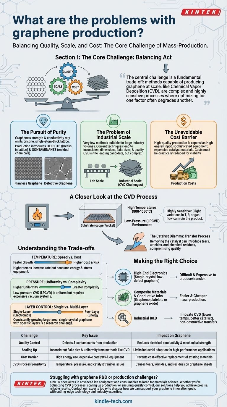
At its core, the primary obstacle to the widespread use of graphene is the immense difficulty in mass-producing a high-quality material at a low cost. While lab-scale methods can create nearly perfect graphene, the existing processes for industrial-scale production struggle to consistently achieve the required purity, structural integrity, and economic viability.
The central challenge is a fundamental trade-off: methods capable of producing graphene at scale, like Chemical Vapor Deposition (CVD), are complex and highly sensitive processes where optimizing for one factor—such as speed or volume—often degrades another, like quality or cost.
The Core Challenge: Balancing Quality, Scale, and Cost
The promise of graphene rests on its flawless atomic structure. Any deviation from this perfection degrades its remarkable properties. The production challenge is a constant balancing act between three competing factors.
The Pursuit of Purity and Perfection
Graphene's strength and conductivity are tied to its pristine, single-atom-thick lattice. Production methods, however, can introduce defects and contaminants.
These imperfections, such as breaks in the lattice or residual chemicals from the manufacturing process, act as roadblocks for electrons and weak points in the material's structure, significantly diminishing its performance.
The Problem of Industrial Scale
While many methods can produce small amounts of graphene, very few are suitable for the large volumes required by industry.
Current techniques often result in material with inconsistent dimensions, flake sizes, and quality levels. Chemical Vapor Deposition (CVD) is the leading candidate for scale, but it is far from a simple "plug-and-play" solution.
The Unavoidable Cost Barrier
High-quality graphene production is an expensive endeavor. The processes demand high energy input, sophisticated equipment, and often rely on expensive catalyst materials.
These costs must be drastically reduced for graphene to become a viable replacement for materials like silicon in electronics or a common additive in composites.
A Closer Look at the CVD Process
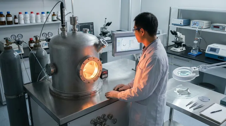
Chemical Vapor Deposition is the most promising method for producing large, continuous sheets of graphene, but it is exceptionally delicate and fraught with technical hurdles.
A Highly Sensitive Environment
The CVD process involves flowing hydrocarbon gases over a catalyst substrate at extremely high temperatures, typically between 800°C and 1050°C.
Controlling this environment is paramount. Most systems use low-pressure chambers (LPCVD) to prevent unwanted gas-phase reactions and ensure the graphene layer deposits with a uniform thickness. Even slight variations in temperature, pressure, or gas flow can ruin the final product.
The Catalyst Dilemma
CVD requires a catalyst, typically a metal like copper or nickel, for the graphene to form on. After growth, this catalyst layer must be removed.
This transfer process is a major source of potential problems. Etching away the metal can introduce tears, wrinkles, and chemical residues onto the fragile graphene sheet, compromising the very quality the CVD process was meant to achieve.
Understanding the Trade-offs
Every decision in the graphene production process involves a compromise, and understanding these is key to appreciating the overall challenge.
Temperature: Speed vs. Cost
Higher temperatures generally increase the reaction rate, allowing for faster graphene growth.
However, operating at over 1000°C consumes massive amounts of energy and places extreme stress on the equipment, increasing both operational costs and the risk of system failure.
Pressure: Uniformity vs. Complexity
Low-pressure CVD is favored for producing highly uniform, single-layer graphene, which is critical for electronics.
This, however, requires complex and expensive vacuum chamber systems. Atmospheric-pressure CVD (APCVD) is simpler and cheaper but makes it much harder to control the growth uniformity.
Layer Control: Single vs. Multi-Layer
For many electronic applications, a perfect single layer of graphene is the goal. For others, like energy storage, precisely controlled few-layer graphene is ideal.
CVD has been optimized for growing large, single-layer sheets. Consistently growing large-area, single-crystal graphene with a specific number of layers remains a significant and unsolved research challenge.
Making the Right Choice for Your Goal
The "best" graphene production method depends entirely on the intended application, as different use cases can tolerate different levels of quality and cost.
- If your primary focus is high-end electronics: You must use single-crystal, low-defect graphene, which is currently the most difficult and expensive to produce and transfer without damage.
- If your primary focus is composite materials or conductive inks: You can likely use graphene platelets or graphene oxide, which have more defects but are far easier and cheaper to mass-produce via methods other than CVD.
- If your primary focus is industrial R&D: The goal is to innovate the CVD process by lowering temperatures, finding better catalysts, or developing a reliable, non-destructive transfer method.
Solving these fundamental production challenges is the final frontier separating graphene's theoretical promise from its real-world technological impact.
Summary Table:
| Challenge | Key Issue | Impact on Graphene |
|---|---|---|
| Quality Control | Defects & contaminants from production | Reduces electrical conductivity & mechanical strength |
| Scaling Up | Inconsistent flake size & uniformity from methods like CVD | Limits industrial adoption for high-performance applications |
| Cost Barrier | High energy use, expensive catalysts & equipment | Prevents cost-effective replacement of existing materials |
| CVD Process Sensitivity | Temperature, pressure, and catalyst transfer issues | Causes tears, wrinkles, and residues on graphene sheets |
Struggling with graphene R&D or production challenges? KINTEK specializes in advanced lab equipment and consumables tailored for materials science. Whether you're optimizing CVD processes, scaling up production, or ensuring quality control, our solutions help you achieve precise, reliable results. Contact our experts today to discuss how we can support your graphene innovation goals with cutting-edge technology and industry expertise.
Visual Guide
Related Products
- HFCVD Machine System Equipment for Drawing Die Nano-Diamond Coating
- Customer Made Versatile CVD Tube Furnace Chemical Vapor Deposition Chamber System Equipment
- Chemical Vapor Deposition CVD Equipment System Chamber Slide PECVD Tube Furnace with Liquid Gasifier PECVD Machine
- Multi Heating Zones CVD Tube Furnace Machine Chemical Vapor Deposition Chamber System Equipment
- Microwave Plasma Chemical Vapor Deposition MPCVD Machine System Reactor for Lab and Diamond Growth
People Also Ask
- What is the chemical vapor deposition growth process? Build Superior Thin Films from the Atom Up
- What are the disadvantages and challenges of the HFCVD method? Overcome Growth Limits and Filament Issues
- What is the hot filament chemical vapour deposition of diamond? A Guide to Synthetic Diamond Coating
- Why is Chemical Vapor Deposition (CVD) equipment uniquely suited for constructing hierarchical superhydrophobic structures?
- What types of substrates are used in CVD to facilitate graphene films? Optimize Graphene Growth with the Right Catalyst


