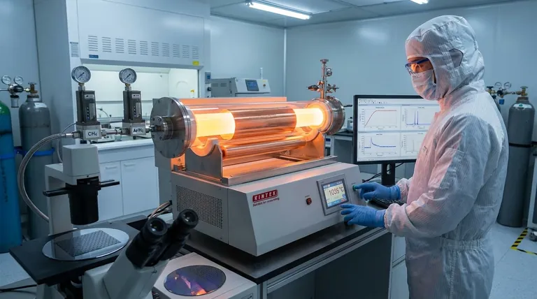
While several methods exist for producing graphene, the dominant technique for synthesizing large-area, high-quality films is Chemical Vapor Deposition (CVD). This bottom-up approach involves growing graphene directly onto a catalytic metal surface from a carbon-based gas at high temperatures. The result is a continuous, single-atom-thick sheet that can then be transferred to a substrate of interest for applications in electronics, materials science, and beyond.
The challenge in graphene synthesis is not just creating the material, but controlling its quality over large areas. While Chemical Vapor Deposition (CVD) is the leading method, its success hinges on meticulously managing the growth environment, particularly the substrate and reaction kinetics.
Deconstructing Chemical Vapor Deposition (CVD)
CVD has become the industry standard because it allows for the scalable production of high-quality, monolayer graphene sheets, which is critical for most electronic and research applications.
The Core Principle: Bottom-Up Growth
CVD is a "bottom-up" synthesis method. Instead of exfoliating layers from a larger piece of graphite, it builds the graphene sheet atom by atom on a surface.
This is achieved by introducing a carbon-containing gas, such as methane (CH₄), into a high-temperature furnace containing a catalytic substrate. The heat causes the gas to decompose, and the carbon atoms arrange themselves into the hexagonal lattice structure of graphene on the substrate's surface.
Key Components of the Process
The success of CVD depends on a few critical components. The most common substrate is a thin foil of a transition metal, with copper (Cu) being particularly popular for growing monolayer graphene.
The entire reaction occurs at very high temperatures, which provides the energy needed for the chemical reactions to proceed and for the carbon atoms to form a crystalline film.
The Critical Transfer Step
A crucial, and often challenging, part of the process is that the graphene is grown on the metal foil, not on its final target substrate. After growth, the delicate, one-atom-thick graphene sheet must be carefully transferred from the metal catalyst to another substrate, like silicon dioxide or a flexible polymer.
Optimizing Graphene Quality
The theoretical perfection of graphene is rarely achieved in practice. Most research in CVD synthesis now focuses on minimizing defects and maximizing crystal size by fine-tuning the growth process.
The Decisive Role of the Substrate
The quality of the final graphene film is highly dependent on the surface it grows on. Scientists now pre-treat the copper foil to prepare it for growth.
This chemical treatment can reduce unwanted catalytic activity and rearrange the surface morphology of the copper. This preparation facilitates the growth of larger, more perfect graphene flakes with fewer imperfections.
Controlling Growth Parameters
Beyond the substrate, several process variables must be precisely controlled. These include the reaction temperature and the transport kinetics of the gas source.
Researchers use partial growth studies to gain insight. By stopping the deposition before individual graphene islands merge into a full sheet, they can study how different parameters affect crystal shape, orientation, and defect density, allowing them to optimize the full process.
Variants of CVD
The most common method is Thermal CVD, which relies solely on high temperatures. However, other variants like Plasma-Enhanced CVD (PECVD) are also used, which can sometimes allow for lower growth temperatures.
Understanding the Trade-offs of CVD
While powerful, CVD is not without its challenges. Objectively understanding its limitations is key to successful implementation.
Complexity and Precision
CVD is not a simple process. It requires sophisticated equipment to maintain high temperatures and vacuum conditions, as well as precise control over gas flow rates. Achieving consistent, high-quality results requires significant expertise and process optimization.
The Transfer-Induced Defect Problem
The transfer process is the Achilles' heel of CVD graphene. Moving a large-area, single-atom-thick film without introducing tears, wrinkles, or contamination is exceptionally difficult. These transfer-induced defects can degrade the material's exceptional electronic properties.
Scalability vs. Cost
CVD allows for the growth of graphene over large areas (e.g., entire metal foils). However, the high-temperature requirements and need for specialized vacuum equipment can make the process relatively expensive compared to methods that produce lower-quality graphene powders.
How to Apply This to Your Project
Your choice of synthesis approach depends entirely on your end goal. There is no single "best" method, only the most appropriate one for a specific application.
- If your primary focus is high-performance electronics: CVD is the standard for producing the required large-area, continuous films, but you must invest heavily in perfecting both the growth and transfer steps.
- If your primary focus is fundamental research on growth mechanics: Partial growth studies are essential for understanding how to control nucleation density and crystal quality at the most basic level.
- If your primary focus is creating composite materials or inks: Other methods not detailed here, such as liquid-phase exfoliation, might be more cost-effective for producing graphene flakes in bulk, where perfect crystallinity is less critical.
Mastering the synthesis of graphene is the fundamental gateway to unlocking its revolutionary potential.
Summary Table:
| Method | Key Feature | Primary Use |
|---|---|---|
| Chemical Vapor Deposition (CVD) | Bottom-up growth on a metal catalyst (e.g., copper) | High-quality, large-area films for electronics |
| Thermal CVD | Relies on high temperatures | Standard process for monolayer graphene |
| Plasma-Enhanced CVD (PECVD) | Can enable lower growth temperatures | Alternative for specific substrate requirements |
Ready to integrate high-quality graphene into your research or product development? KINTEK specializes in providing the advanced lab equipment and expert support needed for sophisticated material synthesis like CVD. Whether you are scaling up production or optimizing growth parameters, our solutions are designed to help you achieve superior results. Contact our experts today to discuss how we can support your specific laboratory needs and accelerate your innovation.
Visual Guide

Related Products
- Chemical Vapor Deposition CVD Equipment System Chamber Slide PECVD Tube Furnace with Liquid Gasifier PECVD Machine
- Customer Made Versatile CVD Tube Furnace Chemical Vapor Deposition Chamber System Equipment
- HFCVD Machine System Equipment for Drawing Die Nano-Diamond Coating
- Split Chamber CVD Tube Furnace with Vacuum Station Chemical Vapor Deposition System Equipment Machine
- Multi Heating Zones CVD Tube Furnace Machine Chemical Vapor Deposition Chamber System Equipment
People Also Ask
- What is plasma enhanced chemical vapor deposition PECVD equipment? A Guide to Low-Temperature Thin Film Deposition
- What are the advantages of chemical vapor deposition? Achieve Superior Thin Films for Your Lab
- What are the processes of vapor phase deposition? Understand CVD vs. PVD for Superior Thin Films
- How are carbon nanotubes grown? Master Scalable Production with Chemical Vapor Deposition
- Why is Chemical Vapor Deposition (CVD) equipment uniquely suited for constructing hierarchical superhydrophobic structures?


