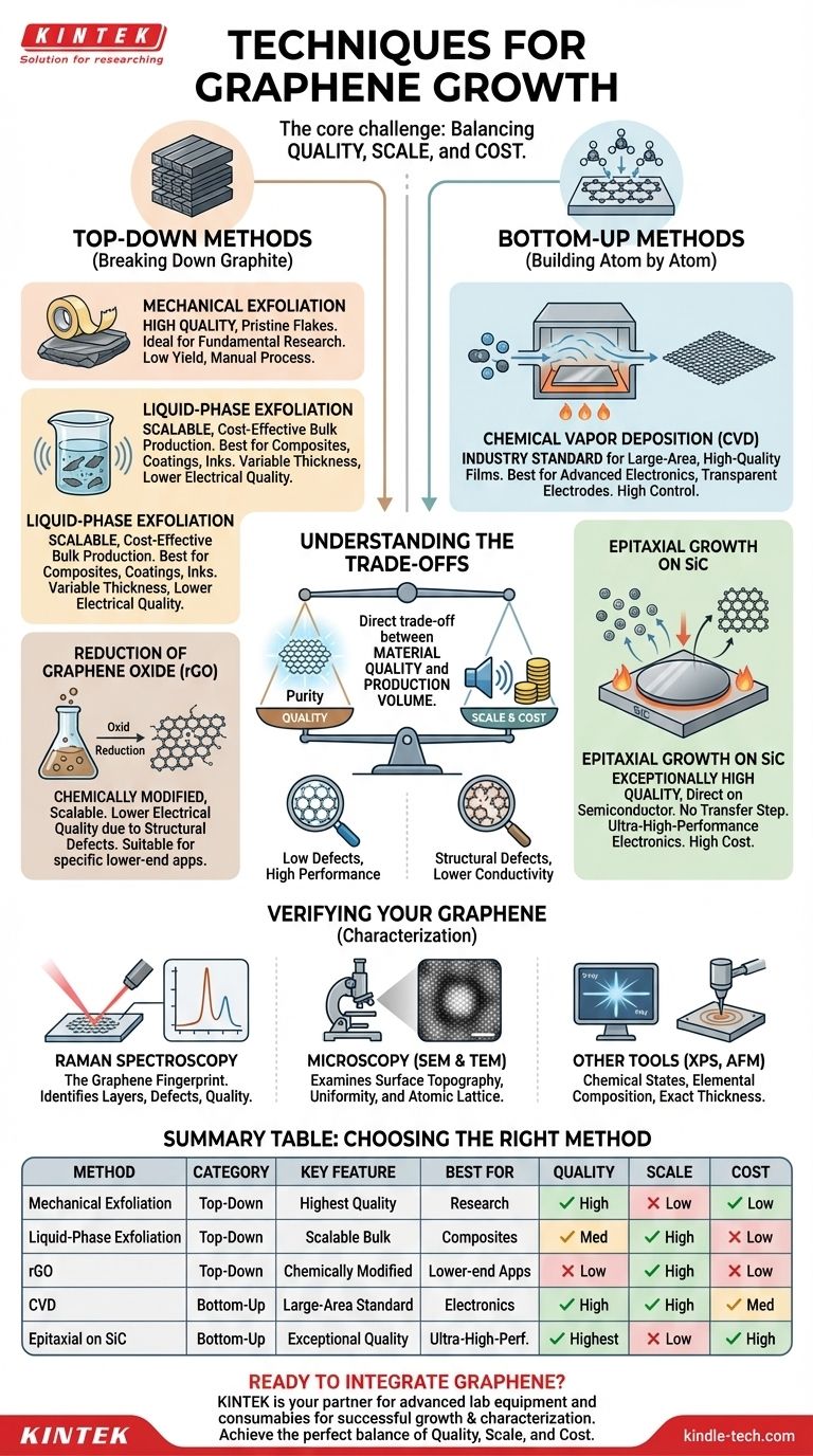
The primary techniques for producing graphene fall into two main categories: "top-down" methods, which start with graphite and break it down, and "bottom-up" methods, which build graphene atom by atom. Key examples include mechanical exfoliation for research, liquid-phase exfoliation for bulk production, and Chemical Vapor Deposition (CVD), which has emerged as the most promising technique for creating the large-area, high-quality graphene needed for advanced electronics.
The core challenge in graphene production is not simply creating it, but creating it with the right balance of quality, scale, and cost for a specific application. No single method is universally "best"; the optimal choice is entirely dependent on the end goal.
Top-Down vs. Bottom-Up: Two Fundamental Philosophies
To understand graphene synthesis, it's essential to grasp the two opposing strategies. The method you choose fundamentally dictates the properties and potential applications of the final material.
What are Top-Down Methods?
Top-down approaches begin with a bulk source of carbon, almost always graphite, which is essentially a stack of countless graphene layers. The goal is to separate these layers.
These methods are conceptually simple but often struggle to produce pristine, defect-free single-layer graphene at scale.
What are Bottom-Up Methods?
Bottom-up synthesis is a constructive process. It starts with atomic carbon precursors—typically in a gaseous form—and assembles them into a single, continuous graphene lattice on a substrate.
This approach offers far greater control over the final structure, enabling the production of high-quality, large-area films.
A Closer Look at Top-Down Techniques
These methods are valued for their low cost and potential for high-volume production, though often at the expense of quality.
Mechanical Exfoliation
This is the original "Scotch tape" method first used to isolate graphene. A piece of tape is used to peel layers from a graphite crystal repeatedly until a single layer remains.
It produces extremely high-quality, pristine graphene flakes ideal for fundamental research. However, it is a manual, low-yield process that is impossible to scale for industrial use.
Liquid-Phase Exfoliation
In this method, graphite powder is mixed into a liquid and subjected to high-energy processes like sonication. This force overcomes the bonds holding the layers together, creating a dispersion of graphene flakes.
This technique is highly scalable and cost-effective for producing large quantities of graphene. The resulting material, however, consists of small flakes with variable thickness and lower electrical quality, making it suitable for composites, coatings, and inks, but not for electronics.
Reduction of Graphene Oxide (rGO)
This is a multi-step chemical process. Graphite is first oxidized to produce graphene oxide (GO), a material rich in oxygen-containing functional groups that is easily dispersed in water. The GO is then chemically or thermally "reduced" to remove most of the oxygen, yielding reduced graphene oxide (rGO).
Like liquid-phase exfoliation, this method is scalable for bulk production. However, the reduction process is imperfect and leaves behind structural defects that degrade the material's electrical properties.
Mastering Bottom-Up Synthesis
Bottom-up methods are the cornerstone of producing graphene for high-performance applications like semiconductors and transparent electrodes.
Chemical Vapor Deposition (CVD)
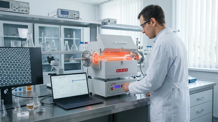
CVD is the leading technique for producing high-quality graphene at a large scale. The process involves heating a substrate, typically a copper or nickel foil, in a vacuum furnace and introducing a carbon-containing gas like methane.
At high temperatures, the gas decomposes, and carbon atoms arrange themselves into a single, continuous layer of graphene on the surface of the metal foil. The graphene can then be transferred to another substrate (like silicon or glass) for use in devices. CVD is the industry standard for electronics applications.
Epitaxial Growth on Silicon Carbide (SiC)
This method involves heating a single-crystal SiC wafer to extremely high temperatures (over 1,300 °C) in a vacuum. The heat causes silicon atoms to sublime (turn into a gas) from the surface, leaving behind carbon atoms that restructure into a layer of graphene.
This technique produces exceptionally high-quality graphene directly on a semiconducting substrate, eliminating the need for a transfer step. However, the process is limited by the high cost and size constraints of SiC wafers.
Understanding the Trade-offs
Choosing a synthesis method requires a clear understanding of its inherent compromises.
The Quality vs. Scale Dilemma
There is a direct trade-off between material quality and production volume. Mechanical exfoliation produces near-perfect graphene but in microscopic quantities. Conversely, liquid-phase exfoliation can produce tons of material, but its quality is significantly lower.
Purity and Defects
Top-down methods, especially the chemical reduction of GO, inevitably introduce structural defects that disrupt the perfect hexagonal lattice of graphene. These defects harm electrical and thermal conductivity.
Bottom-up methods like CVD can produce highly crystalline, low-defect graphene, but their quality is extremely sensitive to process parameters like temperature, gas flow, and substrate purity.
The Role of Cost
Cost is a defining factor. Liquid-phase exfoliation is relatively inexpensive. CVD requires significant capital investment in specialized equipment. Epitaxial growth on SiC is the most expensive method due to the prohibitive cost of the SiC wafers themselves.
Verifying Your Graphene: Essential Characterization
Once graphene is synthesized, its quality must be verified using specialized analytical tools.
Raman Spectroscopy: The Graphene Fingerprint
This is the most critical tool for graphene analysis. It uses a laser to identify the number of graphene layers, assess the level of defects, and confirm the material's quality without destroying the sample.
Microscopy (SEM & TEM)
Scanning Electron Microscopy (SEM) is used to examine the surface topography and uniformity of the graphene film over large areas.
Transmission Electron Microscopy (TEM) provides high-magnification images that can reveal the atomic lattice itself, allowing for direct observation of the crystal structure and defects.
Other Analytical Tools
X-ray Photoelectron Spectroscopy (XPS) is used to characterize the chemical states and elemental composition, which is particularly important for analyzing rGO. Atomic Force Microscopy (AFM) can be used to measure the exact thickness of a graphene flake to confirm it is a single layer.
Choosing the Right Growth Method for Your Goal
Your choice must be guided by your specific objective. There is no one-size-fits-all solution.
- If your primary focus is fundamental research: Mechanical exfoliation provides the highest quality samples for studying intrinsic properties.
- If your primary focus is large-scale electronics: Chemical Vapor Deposition (CVD) is the only viable method for producing large, uniform, high-quality sheets.
- If your primary focus is bulk composites, inks, or coatings: Liquid-phase exfoliation or reduction of graphene oxide offers a cost-effective path to mass production where pristine electrical quality is not critical.
- If your primary focus is ultra-high-performance electronics with a large budget: Epitaxial growth on SiC yields exceptionally high-quality graphene, but at a significant cost premium.
Ultimately, selecting the correct graphene synthesis technique is a strategic decision that aligns the material's properties with the specific demands of your application.
Summary Table:
| Method | Category | Key Feature | Best For |
|---|---|---|---|
| Mechanical Exfoliation | Top-Down | Highest Quality, Pristine Flakes | Fundamental Research |
| Liquid-Phase Exfoliation | Top-Down | Scalable, Cost-Effective Bulk Production | Composites, Coatings, Inks |
| Reduction of Graphene Oxide (rGO) | Top-Down | Chemically Modified, Scalable | Applications where lower electrical quality is acceptable |
| Chemical Vapor Deposition (CVD) | Bottom-Up | Industry Standard for Large-Area, High-Quality Films | Electronics, Transparent Electrodes |
| Epitaxial Growth on SiC | Bottom-Up | Exceptionally High Quality, No Transfer Needed | Ultra-High-Performance Electronics (High Cost) |
Ready to Integrate Graphene into Your Research or Production?
Navigating the complexities of graphene synthesis requires the right tools and expertise. Whether you are developing next-generation electronics with CVD or scaling up composite materials, KINTEK is your partner for advanced lab equipment and consumables.
We specialize in providing the precise, reliable equipment needed for successful graphene growth and characterization, helping you achieve the perfect balance of quality, scale, and cost for your specific application.
Contact our experts today to discuss how our solutions can accelerate your graphene innovation.
Visual Guide
Related Products
- CVD Diamond Dressing Tools for Precision Applications
- Multi Heating Zones CVD Tube Furnace Machine Chemical Vapor Deposition Chamber System Equipment
- CVD Diamond Domes for Industrial and Scientific Applications
- CVD Diamond for Thermal Management Applications
- Chemical Vapor Deposition CVD Equipment System Chamber Slide PECVD Tube Furnace with Liquid Gasifier PECVD Machine
People Also Ask
- What are the raw materials for CVD diamonds? A seed, a gas, and the science of crystal growth.
- How do you identify a CVD diamond? The Definitive Guide to Lab-Grown Diamond Verification
- What color diamonds are CVD? Understanding the Process from Brown Tint to Colorless Beauty
- What is CVD diamond? The Ultimate Guide to Lab-Grown Diamonds and Their Uses
- How long does it take to make synthetic diamonds? Discover the 6-8 Week Science Behind Lab-Grown Gems


