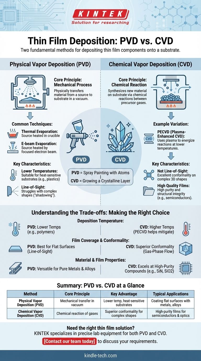
At the highest level, the two fundamental methods for depositing thin film components onto a substrate are Physical Vapor Deposition (PVD) and Chemical Vapor Deposition (CVD). These two categories represent entirely different approaches to building a film. PVD is a mechanical process that physically transfers material from a source to the substrate, while CVD uses chemical reactions between precursor gases to grow a new material directly on the substrate's surface.
The core distinction is not about which method is better, but about the mechanism of creation. Think of PVD as spray painting with atoms in a vacuum, while CVD is like growing a crystalline layer on a surface through a controlled chemical reaction.
What is Physical Vapor Deposition (PVD)?
Physical Vapor Deposition encompasses a family of techniques where a material is converted into a vapor phase, transported across a vacuum chamber, and condensed onto a substrate as a thin film. The composition of the film is the same as the source material.
The Core Principle: A Mechanical Process
PVD is fundamentally a line-of-sight process. Atoms or molecules are liberated from a solid source material (known as a "target") and travel in a straight line to coat whatever is in their path.
This entire process must occur in a high-vacuum environment to ensure the vaporized atoms can travel without colliding with air molecules.
Common PVD Techniques
Two of the most common PVD methods are thermal evaporation and e-beam evaporation.
In thermal evaporation, the source material is heated in a small crucible until it evaporates, creating a vapor cloud that coats the substrate.
E-beam (electron beam) evaporation uses a high-energy, focused beam of electrons to heat the source material, offering more precise control and the ability to evaporate materials with very high melting points.
Key Characteristics of PVD
PVD processes are generally performed at lower temperatures compared to CVD. This makes them highly suitable for depositing films on temperature-sensitive substrates, such as plastics.
Because it is a line-of-sight technique, PVD can struggle to uniformly coat complex, three-dimensional shapes, an effect known as "shadowing."
What is Chemical Vapor Deposition (CVD)?
Chemical Vapor Deposition is a process where the substrate is exposed to one or more volatile precursor gases. These gases react or decompose on the substrate's surface to produce the desired thin film.
The Core Principle: A Chemical Reaction
Unlike PVD, CVD does not physically transfer an existing material. Instead, it synthesizes an entirely new solid material directly on the substrate through a chemical reaction.
The excess gases and reaction byproducts are exhausted from the chamber, leaving behind a highly pure and dense film.
An Example: Plasma-Enhanced CVD (PECVD)
A common variation is Plasma-Enhanced Chemical Vapor Deposition (PECVD). This method uses plasma—a state of matter with free electrons and ions—to energize the precursor gases.
This plasma allows the necessary chemical reactions to occur at much lower temperatures than in traditional thermal CVD, broadening the range of compatible substrates.
Key Characteristics of CVD
CVD is not a line-of-sight process. The precursor gases can flow around complex geometries, resulting in excellent conformality—the ability to create a highly uniform coating on intricate surfaces.
The films produced by CVD are often very high quality, with excellent purity and structural integrity, making them critical for applications in semiconductors and advanced optics.
Understanding the Trade-offs: PVD vs. CVD
Choosing between these methods requires a clear understanding of their respective strengths and limitations.
Deposition Temperature and Substrate
PVD's lower process temperatures provide a significant advantage when working with substrates that cannot withstand high heat, like polymers or certain electronic components.
Traditional CVD requires high temperatures to drive the chemical reactions, though techniques like PECVD help mitigate this constraint.
Film Coverage and Conformality
CVD is the clear choice for coating complex shapes or deep trenches. Its gas-phase nature ensures a uniform, conformal layer.
PVD is best suited for coating relatively flat surfaces, where its line-of-sight deposition is not a hindrance.
Material and Film Properties
PVD is extremely versatile for depositing a wide range of pure metals, alloys, and compounds without altering their chemical makeup.
CVD excels at creating specific, high-purity compounds like silicon nitride or silicon dioxide, which are fundamental building blocks in the microelectronics industry.
Making the Right Choice for Your Goal
Your choice depends entirely on the material you need to deposit, the shape and thermal sensitivity of your substrate, and the final properties required of the film.
- If your primary focus is coating a heat-sensitive substrate or a simple, flat surface with metal: PVD is often the more direct, versatile, and cost-effective approach.
- If your primary focus is creating a highly pure, uniform, and dense film on a complex 3D shape: CVD provides superior conformality and film quality, provided the substrate can handle the process conditions.
Understanding the fundamental difference between these physical and chemical pathways is the first step to mastering thin film technology.
Summary Table:
| Method | Core Principle | Key Advantage | Typical Applications |
|---|---|---|---|
| Physical Vapor Deposition (PVD) | Mechanical transfer of material in a vacuum | Lower temperature, ideal for heat-sensitive substrates | Coating flat surfaces with metals, alloys, and compounds |
| Chemical Vapor Deposition (CVD) | Chemical reaction of gases on the substrate surface | Superior conformality for complex 3D shapes | Creating high-purity films for semiconductors and optics |
Need to choose the right thin film deposition method for your project?
KINTEK specializes in providing the precise lab equipment and consumables you need for both PVD and CVD processes. Whether you're working with temperature-sensitive materials or require a highly conformal coating, our experts can help you select the ideal solution to achieve superior film quality and performance.
Contact our team today to discuss your specific application requirements and discover how KINTEK can support your laboratory's thin film technology goals.
Visual Guide
Related Products
- Tungsten Evaporation Boat for Thin Film Deposition
- Custom CVD Diamond Coating for Lab Applications
- Aluminized Ceramic Evaporation Boat for Thin Film Deposition
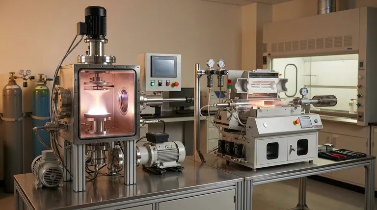
- Chemical Vapor Deposition CVD Equipment System Chamber Slide PECVD Tube Furnace with Liquid Gasifier PECVD Machine
- Electron Beam Evaporation Coating Oxygen-Free Copper Crucible and Evaporation Boat
People Also Ask
- What is the difference between PVD and CVD? Choose the Right Thin-Film Deposition Technique
- What is the process of thin film deposition? A Guide to PVD, CVD, and Coating Techniques
- What is a thin film evaporator? A Gentle Solution for Heat-Sensitive & Viscous Materials
- What is the layer method of deposition? A Guide to PVD vs. CVD Thin-Film Techniques
- What methods are used to deposit thin films? A Guide to PVD, CVD, and ALD Techniques


