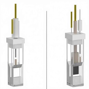
Thin films are microscopic layers of material with thicknesses ranging from fractions of a nanometer to several micrometers. far from being simple surface coverings, they are critical components utilized in applications ranging from industrial coatings and energy conversion systems to advanced memory storage devices.
Thin films act as high-precision interfaces that modify the optical, electrical, and mechanical behavior of surfaces without the bulk of solid materials, enabling the conservation of scarce resources while unlocking new engineering capabilities.
The Architecture of Thin Films
Variable Composition
Depending on the required properties, a thin film can be a single homogeneous layer. This type features a uniform composition with a single crystalline phase and microstructure.
Complex Multilayer Structures
Alternatively, films can be engineered as inhomogeneous multilayer or composite structures. These complex architectures may be periodic (following a set pattern) or entirely random, allowing for sophisticated manipulation of material properties.
Material Diversity
A wide variety of materials can be utilized to create these films. Common choices include metals, ceramics, polymers, and carbon-based compounds, selected specifically to match the intended function of the final product.
Key Functional Properties
Optical Control
Thin films are essential for creating optical coatings. They improve device performance by reducing reflection and scattering, while simultaneously protecting sensitive components from dust and moisture.
Electrical Precision
In the semiconductor industry, films serve as barriers or contacts with strictly controlled thicknesses. This allows engineers to dictate specific electronic properties, such as insulation or conductivity, which are vital for microelectronic components.
Surface Protection
Beyond electronics, thin films provide physical durability. They grant surfaces resistance to wear and corrosion, extending the lifespan of materials and optical components.
Applications in Modern Technology
Consumer Electronics and Displays
Thin films power the mobile devices and healthcare equipment used daily. In LED manufacturing, films of light-emitting or light-absorbing materials determine the display’s color and brightness.
Energy and Storage
These films are central to renewable energy, specifically in thin-film photovoltaic cells that convert light to power. They are also utilized in thin-film batteries and data storage devices.
Specialized Sensors
The versatility of thin films extends to biosensors and plasmonic devices. They facilitate high-tech applications where interaction at the molecular level is required.
Strategic Advantages and Engineering Implications
Conservation of Resources
One of the primary engineering benefits of thin films is the conservation of scarce materials. Because the layers are microscopic, high-value materials can be used sparingly without sacrificing performance.
Ecological Benefits
The production of thin films often leads to reduced effluent output and lower power consumption. This makes them a more environmentally friendly alternative to traditional bulk material processing.
Solving Engineering Paradoxes
Thin films enable the creation of nanostructured coatings and nanocomposites. These advancements offer solutions to previously unsolved engineering problems, facilitating the creation of revolutionary products that were not possible with bulk materials.
Making the Right Choice for Your Goal
To leverage thin films effectively, you must align the material choice with your specific performance criteria.
- If your primary focus is Efficiency: Prioritize thin films to conserve scarce materials and reduce the power consumption of your manufacturing process.
- If your primary focus is Performance: Utilize multilayer or composite structures to achieve precise optical transmission or electrical insulation properties unavailable in bulk materials.
- If your primary focus is Durability: Implement ceramic or metallic films to provide robust resistance against wear, corrosion, and environmental moisture.
Thin films transform ordinary surfaces into highly functional, efficient, and intelligent components.
Summary Table:
| Feature | Description | Key Benefits |
|---|---|---|
| Thickness Range | Fractions of a nanometer to several micrometers | Material conservation & microscopic precision |
| Composition | Metals, Ceramics, Polymers, Carbon-based compounds | Versatile functionality and material diversity |
| Structure | Single layer or complex multilayer/composite | Tailored optical and electrical properties |
| Function | Optical control, electrical insulation, surface protection | Enhanced durability and device performance |
| Applications | PV cells, LEDs, semiconductors, biosensors | Energy efficiency and technological innovation |
Elevate Your Research and Production with KINTEK Precision Solutions
Unlock the full potential of thin-film technology with KINTEK’s industry-leading laboratory equipment. Whether you are developing next-generation semiconductors, high-efficiency photovoltaic cells, or advanced biosensors, our comprehensive range of high-temperature vacuum and CVD furnaces, high-pressure reactors, and precision crushing systems ensures you achieve the exact material properties your project demands.
Why partner with KINTEK?
- Unmatched Versatility: From PECVD/MPCVD systems for advanced coatings to pellet presses and crucibles for material preparation.
- Reliable Performance: High-precision tools designed for the rigorous demands of battery research and nanostructured coating development.
- Expert Support: We provide the essential consumables—including PTFE products and ceramics—to keep your lab running at peak efficiency.
Ready to solve your most complex engineering paradoxes? Contact us today to find the perfect equipment for your thin-film applications!
Related Products
- Aluminized Ceramic Evaporation Boat for Thin Film Deposition
- Tungsten Evaporation Boat for Thin Film Deposition
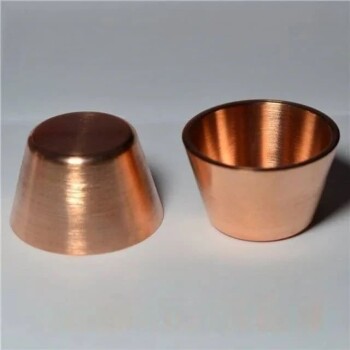
- Electron Beam Evaporation Coating Oxygen-Free Copper Crucible and Evaporation Boat
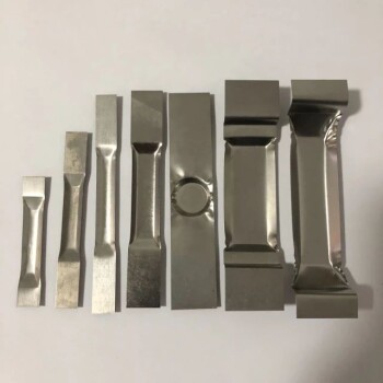
- Molybdenum Tungsten Tantalum Evaporation Boat for High Temperature Applications
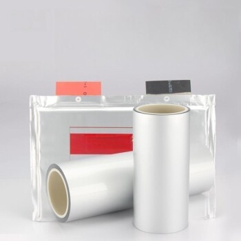
- Aluminum-Plastic Flexible Packaging Film for Lithium Battery Packaging
People Also Ask
- What are the alternatives to sputtering? Choose the Right Thin Film Deposition Method
- Why is an alumina boat and Ti3AlC2 powder bed necessary for Ti2AlC sintering? Protect MAX Phase Purity
- What are thin films deposited by evaporation? A Guide to High-Purity Coating
- What is the chemical method for thin film deposition? Build Films from the Molecular Level Up
- What is the widely used boat made of in thermal evaporation? Choosing the Right Material for High-Purity Deposition

