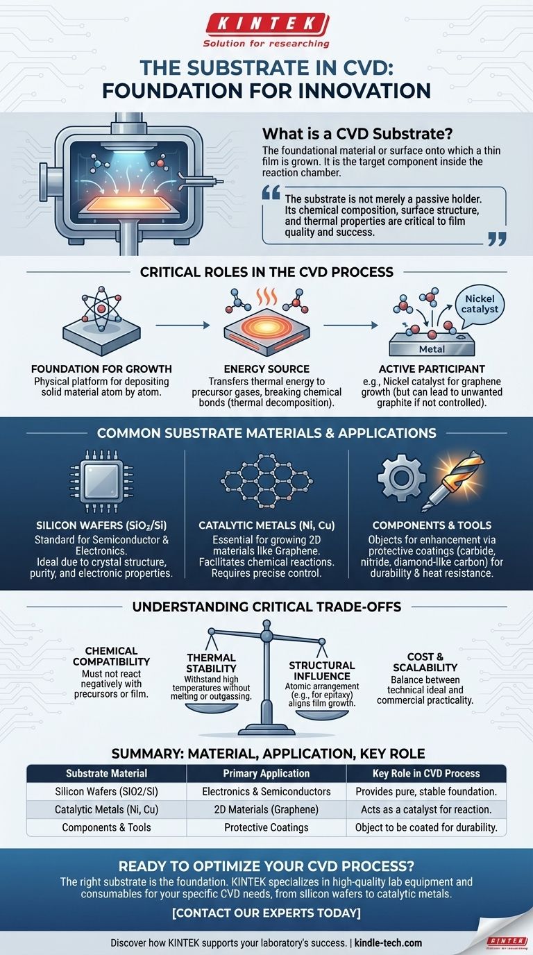
In Chemical Vapor Deposition (CVD), the substrate is the foundational material or surface onto which a thin film is grown. It is the target component inside the reaction chamber that gets coated. For example, to grow graphene, a thin film of nickel can be used as the substrate, or for electronic components, a silicon wafer (SiO2/Si) is often the base material.
The substrate is not merely a passive holder for the final product. Its chemical composition, surface structure, and thermal properties are critical factors that actively influence the chemical reactions and determine the quality, structure, and success of the deposited film.
The Role of the Substrate in the CVD Process
Chemical Vapor Deposition is a process that transforms precursor gases into a solid film on a heated surface. The substrate is that critical surface, and it plays several key roles.
The Foundation for Film Growth
At its most basic, the substrate serves as the physical platform. The entire CVD process is designed to deposit a solid material, atom by atom or molecule by molecule, onto this base.
The reference to a film being deposited "on a heated surface" is referring directly to the substrate.
An Energy Source for the Reaction
The substrate is typically heated to high temperatures. This thermal energy is transferred to the precursor gases that flow over it.
This energy breaks the chemical bonds in the gas molecules, a process called thermal decomposition. The newly freed atoms or molecules then settle and react on the hot substrate surface to form the desired solid film.
An Active Participant in Deposition
A substrate can be more than just a hot surface; it can actively participate in the chemistry of the deposition.
For example, when growing graphene, a nickel substrate can act as a catalyst. However, as the references note, it can also absorb too much carbon, resulting in thick, unwanted graphite instead of a single layer of graphene. This illustrates how the substrate's material properties directly dictate the outcome.
Common Substrate Materials
The choice of substrate is entirely dependent on the film being deposited and the final application. While countless materials can be used, some are common for specific goals.
Silicon Wafers (SiO2/Si)
For the semiconductor and electronics industries, silicon wafers, often with a layer of silicon dioxide (SiO2), are the standard.
Their crystal structure, purity, and well-understood electronic properties make them the ideal foundation for building integrated circuits and other micro-devices.
Catalytic Metals (e.g., Nickel, Copper)
For growing advanced 2D materials like graphene, catalytic metals are required. These metals, such as nickel, not only provide a surface but also facilitate the chemical reaction.
As noted, controlling the properties of these metal substrates, such as using a thin nickel film under 300 nm, is crucial to prevent undesirable side reactions and achieve a high-quality film.
Components and Tools
In many industrial applications, the substrate is the object that needs enhancement. CVD is often used as a coating process to improve durability, reduce friction, or increase heat resistance.
In this case, a machine part, a cutting tool, or a medical implant becomes the substrate that receives the protective carbide, nitride, or diamond-like carbon film.
Understanding the Trade-offs: Substrate Selection is Critical
Choosing the wrong substrate can lead to complete process failure. The decision involves balancing several key factors.
Chemical Compatibility
The substrate material must not react negatively with the precursor gases or the deposited film. The nickel and graphite example is a perfect illustration of this pitfall. A substrate that promotes the wrong chemical pathway will yield an unusable product.
Thermal Stability
CVD processes operate at high temperatures. The substrate must be able to withstand this heat without melting, deforming, or outgassing impurities that would contaminate the film.
Structural Influence
For growing highly ordered, single-crystal films, the atomic arrangement of the substrate surface is paramount. A process known as epitaxy relies on matching the crystal lattice of the substrate to guide the growth of a perfectly aligned film. An incompatible crystal structure will result in a lower-quality polycrystalline or amorphous film.
Cost and Scalability
Finally, practical considerations are key. The ideal technical substrate might be prohibitively expensive or unavailable in the required size or quantity for a commercial application. The final choice is always a trade-off between performance and practicality.
Making the Right Choice for Your Application
Your end goal dictates the correct substrate choice.
- If your primary focus is electronics manufacturing: You will almost certainly use silicon-based substrates (like SiO2/Si) for their purity, scalability, and well-understood integration with semiconductor processes.
- If your primary focus is growing 2D materials like graphene: A catalytic metal substrate like nickel or copper is necessary, but you must precisely control its preparation and thickness to achieve the desired single-layer film.
- If your primary focus is creating durable coatings on tools or parts: The component itself serves as the substrate, and the main concerns are its ability to withstand the process temperature and form a strong bond with the deposited film.
Ultimately, selecting the right substrate is as crucial as choosing the precursor gases, as it defines the foundation upon which your desired material is built.
Summary Table:
| Substrate Material | Primary Application | Key Role in CVD Process |
|---|---|---|
| Silicon Wafers (SiO2/Si) | Electronics & Semiconductors | Provides a pure, stable foundation for micro-devices. |
| Catalytic Metals (Ni, Cu) | 2D Materials (e.g., Graphene) | Acts as a catalyst for the chemical reaction. |
| Components & Tools | Protective Coatings | The object to be coated, enhancing durability or performance. |
Ready to Optimize Your CVD Process?
The right substrate is the foundation of a successful deposition. KINTEK specializes in providing high-quality lab equipment and consumables tailored to your specific CVD application, whether you're working with silicon wafers, catalytic metals, or specialized components. Our expertise ensures you have the right materials for superior film quality and process efficiency.
Contact our experts today to discuss your substrate needs and discover how KINTEK can support your laboratory's success.
Visual Guide
Related Products
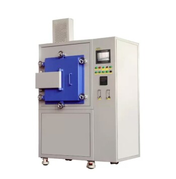
- Customer Made Versatile CVD Tube Furnace Chemical Vapor Deposition Chamber System Equipment
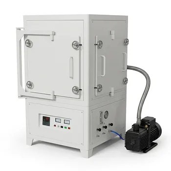
- Multi Heating Zones CVD Tube Furnace Machine Chemical Vapor Deposition Chamber System Equipment
- Horizontal High Temperature Graphite Vacuum Graphitization Furnace
- Vertical High Temperature Graphite Vacuum Graphitization Furnace
- Controlled Nitrogen Inert Hydrogen Atmosphere Furnace
People Also Ask
- What is the difference between hot wall CVD and cold wall CVD? Choose the Right System for Your Process
- What is the temperature of a CVD furnace? From 200°C to 1600°C for Precise Film Deposition
- What is the effect of temperature on graphene oxide? Master Thermal Reduction for Precise Material Properties
- What is the function of a high-temperature CVD tube furnace in 3D graphene foam prep? Master 3D Nanomaterial Growth
- How does a CVD tube furnace inhibit the sintering of silver supports? Boost Membrane Durability and Performance