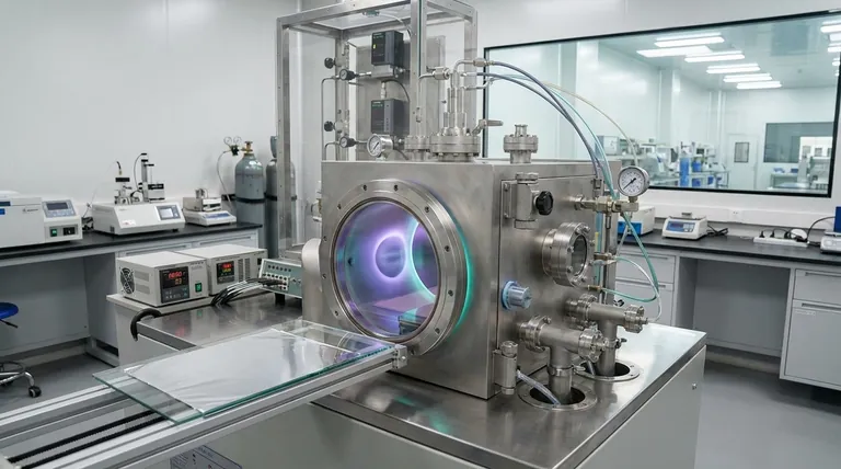
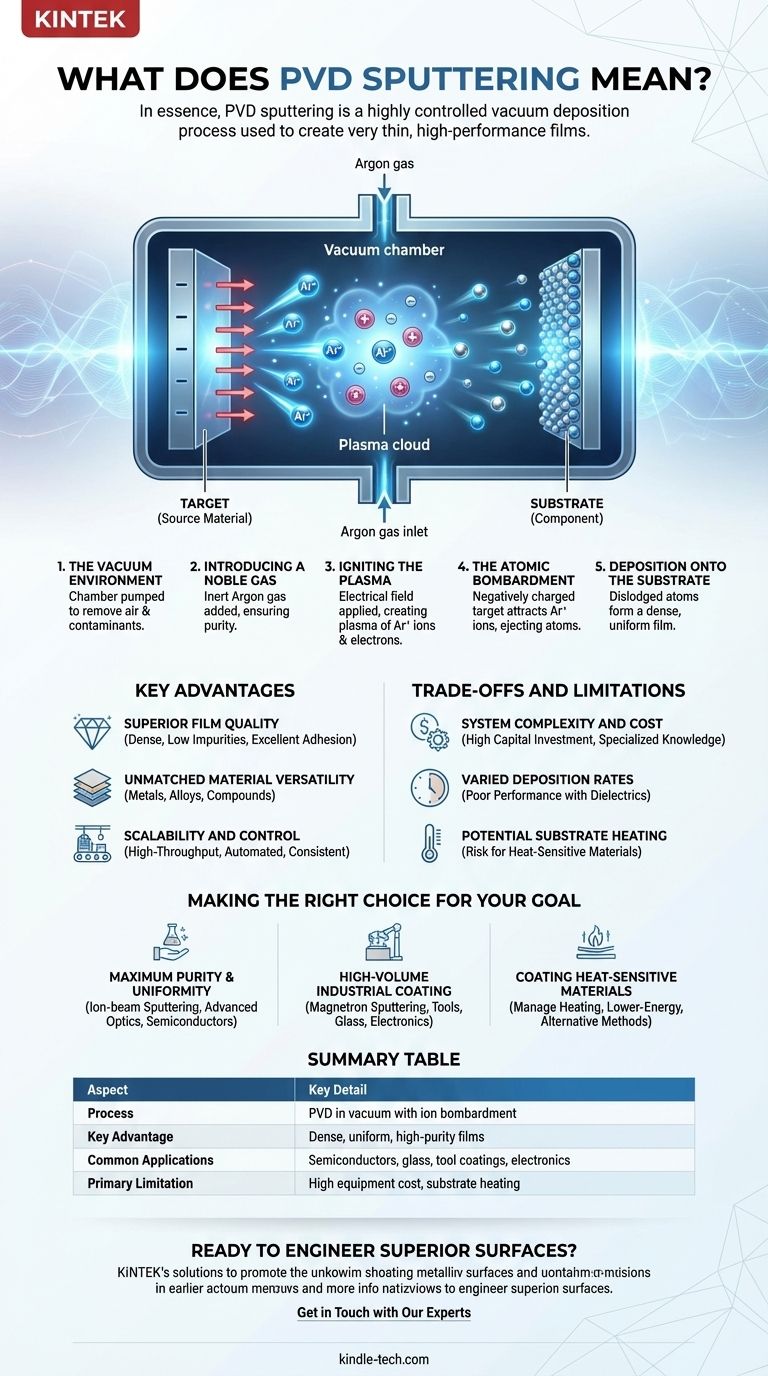
In essence, PVD sputtering is a highly controlled vacuum deposition process used to create very thin, high-performance films. The technique works by bombarding a source material, known as a "target," with high-energy ions. This atomic-scale collision physically knocks off, or "sputters," atoms from the target, which then travel through the vacuum and deposit onto a component, called a "substrate," forming a uniform coating.
The core challenge in many advanced industries is applying an extremely thin, pure, and durable coating onto a surface. PVD sputtering solves this by using a physical, non-thermal method—akin to an atomic-scale sandblasting—to transfer material, resulting in exceptionally dense and uniform films.
How the Sputtering Process Works
To understand sputtering, it’s best to visualize it as a sequence of events occurring within a sealed vacuum chamber. This controlled environment is critical to the quality and purity of the final coating.
The Vacuum Environment
First, the target material and the substrate to be coated are placed inside a vacuum chamber. Air is pumped out to remove oxygen, water vapor, and other particles that could contaminate the film.
Introducing a Noble Gas
Next, a small, controlled amount of an inert gas—most commonly argon—is introduced into the chamber. As a noble gas, argon will not chemically react with the target material, ensuring the deposited film remains pure.
Igniting the Plasma
An electrical field is applied within the chamber, which energizes the argon gas and strips electrons from the argon atoms. This creates a plasma, an ionized state of matter containing positively charged argon ions and free electrons.
The Atomic Bombardment
The target material is given a strong negative electrical charge. This causes the positively charged argon ions from the plasma to accelerate violently towards the target, striking its surface with significant force.
Deposition onto the Substrate
Each collision has enough energy to physically eject atoms from the target material. These dislodged atoms travel in a straight line through the vacuum until they strike the substrate, where they condense and slowly build up a thin, dense film, one atomic layer at a time.
Key Advantages of PVD Sputtering
Sputtering is a standard coating technique in many industries for several distinct reasons, centered on the quality and consistency of the result.
Superior Film Quality
The process creates films that are incredibly dense, with low levels of impurities. This results in coatings with excellent adhesion and durability. Specific methods like ion-beam sputtering can achieve the highest levels of uniformity and purity.
Unmatched Material Versatility
Sputtering can be used to deposit a vast range of materials, including metals, alloys, and compounds. This flexibility allows it to be used for an enormous number of applications across many different industries.
Scalability and Control
The process is highly controllable and can be automated for high-throughput manufacturing. This makes it an economic and reliable choice for large-scale industrial production where consistency is critical.
Understanding the Trade-offs and Limitations
While powerful, PVD sputtering is not the ideal solution for every situation. Understanding its limitations is key to making an informed decision.
System Complexity and Cost
The equipment required for PVD sputtering is sophisticated and represents a significant capital investment. The machinery is complex and requires specialized knowledge to operate and maintain.
Varied Deposition Rates
While sputtering can deposit metals at a high rate, its performance with dielectric (electrically insulating) materials is often poor. This can make the process inefficient for certain applications, such as some optical coatings.
Potential Substrate Heating
The energy transferred during the deposition process can cause the substrate to heat up. This can be a significant issue when coating plastics or other materials that are sensitive to high temperatures.
Making the Right Choice for Your Goal
Selecting the right coating technology depends entirely on the priorities of your project. PVD sputtering offers a spectrum of possibilities tailored to different needs.
- If your primary focus is maximum film purity and uniformity: Ion-beam sputtering is the superior choice for applications where film quality is the absolute highest priority, such as in advanced optics or semiconductors.
- If your primary focus is high-volume industrial coating: Magnetron sputtering provides high deposition rates and excellent scalability, making it a cost-effective standard for coating tools, architectural glass, and electronics.
- If your primary focus is coating a heat-sensitive material: The potential for substrate heating must be carefully managed, and it may be necessary to explore lower-energy sputtering configurations or alternative PVD methods.
Ultimately, PVD sputtering is a foundational technology for engineering the high-performance surfaces that define modern tools, electronics, and scientific instruments.
Summary Table:
| Aspect | Key Detail |
|---|---|
| Process | Physical vapor deposition in a vacuum using ion bombardment. |
| Key Advantage | Produces dense, uniform, and high-purity thin films. |
| Common Applications | Semiconductors, architectural glass, tool coatings, electronics. |
| Primary Limitation | High equipment cost and potential for substrate heating. |
Ready to Engineer Superior Surfaces?
PVD sputtering is the key to creating high-performance, durable coatings for your most critical components. Whether you're developing advanced electronics, precision optics, or wear-resistant tools, the right equipment is essential for success.
KINTEK specializes in advanced lab equipment and consumables, providing the reliable PVD sputtering solutions your laboratory needs. Our expertise ensures you achieve the film purity, adhesion, and consistency required for your projects.
Contact us today to discuss your specific coating challenges and discover how our solutions can enhance your R&D and production capabilities.
Visual Guide
Related Products
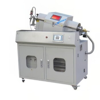
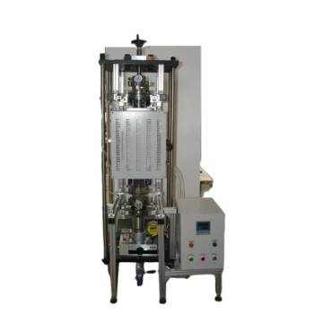
- Inclined Rotary Plasma Enhanced Chemical Vapor Deposition PECVD Equipment Tube Furnace Machine
- RF PECVD System Radio Frequency Plasma-Enhanced Chemical Vapor Deposition RF PECVD
- HFCVD Machine System Equipment for Drawing Die Nano-Diamond Coating
- Inclined Rotary Plasma Enhanced Chemical Vapor Deposition PECVD Equipment Tube Furnace Machine
- Custom CVD Diamond Coating for Lab Applications
People Also Ask
- What is PECVD used for? Achieve Low-Temperature, High-Performance Thin Films
- What materials are deposited in PECVD? Discover the Versatile Thin-Film Materials for Your Application
- What is the difference between PECVD and CVD? Unlock the Right Thin-Film Deposition Method
- What is plasma in CVD process? Lowering Deposition Temperatures for Heat-Sensitive Materials
- How does plasma enhanced CVD work? Achieve Low-Temperature, High-Quality Thin Film Deposition