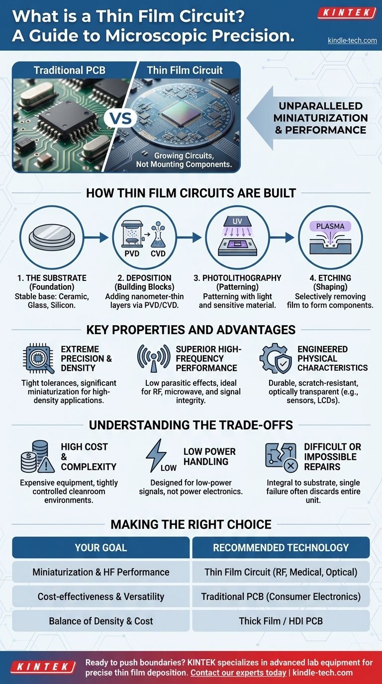
At its core, a thin film circuit is an electronic circuit built by depositing extremely thin layers of conductive, resistive, and insulating materials onto a stable base, or substrate. These films can be just nanometers thick, and they are layered and shaped with incredible precision to form microscopic components like resistors, capacitors, and interconnects directly on the surface.
A thin film circuit is fundamentally different from a traditional circuit board. Instead of mounting separate components onto a board, you are essentially "printing" or "growing" the entire integrated circuit onto a substrate, enabling unparalleled miniaturization and performance for specialized applications.
How Thin Film Circuits Are Built
Understanding a thin film circuit requires understanding its manufacturing process, which is a game of addition and subtraction at a microscopic scale. The process combines material deposition with selective removal to create intricate patterns.
The Foundation: The Substrate
Everything starts with a substrate. This is the physical base upon which the circuit is built. Substrates are chosen for their specific thermal and electrical properties, with common materials including ceramic (like alumina), glass, or silicon.
The Building Blocks: Deposition
Deposition is the process of adding the thin layers of material. The two most common methods are Physical Vapor Deposition (PVD) and Chemical Vapor Deposition (CVD).
- Physical Vapor Deposition (PVD): This involves physically moving a material from a source to the substrate. This is often done through sputtering, where ions bombard a target material, knocking atoms loose that then coat the substrate.
- Chemical Vapor Deposition (CVD): This method uses precursor gases that react on the surface of the substrate when energized (e.g., by heat), forming a solid, thin film.
The choice of deposition method and material directly influences the final properties of the circuit, such as its electrical conductivity or durability.
The Design: Photolithography and Etching
Once a layer is deposited, it must be patterned to create the actual circuit components. This is typically done using photolithography, a process similar to developing film. A light-sensitive material is applied, exposed to a pattern of UV light, and then developed, leaving a protective mask over the desired circuit areas.
Finally, etching processes (like plasma etching) are used to remove the unprotected film material. This leaves behind the precisely shaped conductors, resistors, and other elements that make up the final circuit.
Key Properties and Advantages
The complex manufacturing process yields circuits with unique and powerful characteristics that are impossible to achieve with traditional methods.
Extreme Precision and Density
Because components are defined at a microscopic level, they can have extremely tight tolerances and be packed very closely together. This allows for significant miniaturization and superior performance in high-density applications.
Superior High-Frequency Performance
The small size and precise geometry of thin film components reduce parasitic capacitance and inductance. This makes them ideal for high-frequency applications, such as RF and microwave systems, where signal integrity is critical.
Engineered Physical Characteristics
Thin films can be engineered for more than just electrical properties. They can be made to be highly durable, scratch-resistant, or even optically transparent, which is essential for devices like LCD screens or advanced optical sensors.
Understanding the Trade-offs
Despite their advantages, thin film circuits are not a universal solution. Their specialized nature comes with significant trade-offs that limit their use.
High Cost and Complexity
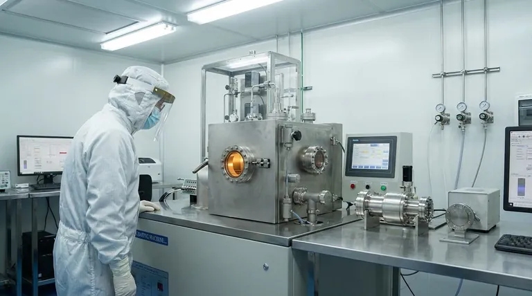
The equipment required for deposition and etching (like PVD and CVD machines) is extremely expensive and must be operated in tightly controlled cleanroom environments. This makes manufacturing far more costly and complex than for standard Printed Circuit Boards (PCBs).
Low Power Handling
The extremely thin nature of the conductive layers means they cannot handle high currents or significant power loads. They are designed for low-power signal processing, not power electronics.
Difficult or Impossible Repairs
Unlike a PCB where a failed component can often be desoldered and replaced, a component on a thin film circuit is an integral part of the substrate. A single point of failure typically means the entire circuit must be discarded.
Making the Right Choice for Your Goal
The decision to use thin film technology depends entirely on your specific engineering priorities and constraints.
- If your primary focus is miniaturization and high-frequency performance: Thin film is the ideal choice for applications like RF modules, optical transceivers, and advanced medical sensors where precision and small form factor are non-negotiable.
- If your primary focus is cost-effectiveness and versatility: Traditional PCBs remain the undisputed standard for the vast majority of electronic products due to their low cost, design flexibility, and ease of assembly.
- If your primary focus is a balance of density and cost: You may investigate "thick film" technology, which is a similar but less precise process, or advanced high-density interconnect (HDI) PCBs.
Ultimately, understanding thin film technology empowers you to select the right tool for the right engineering challenge.
Summary Table:
| Aspect | Thin Film Circuit | Traditional PCB |
|---|---|---|
| Manufacturing | PVD/CVD deposition, photolithography | Etching, component mounting |
| Key Advantage | Extreme miniaturization, high-frequency performance | Cost-effectiveness, versatility |
| Ideal For | RF modules, medical sensors, optical devices | Consumer electronics, general-purpose circuits |
| Power Handling | Low power | High power |
Ready to push the boundaries of your electronic designs with thin film technology?
At KINTEK, we specialize in providing the advanced lab equipment and consumables needed for precise thin film deposition and circuit fabrication. Whether you're developing cutting-edge RF modules, medical sensors, or optical devices, our expertise and high-quality materials can help you achieve unparalleled miniaturization and performance.
Contact our experts today to discuss how we can support your laboratory's specific needs and help you select the right tools for your next breakthrough project.
Visual Guide
Related Products
- Chemical Vapor Deposition CVD Equipment System Chamber Slide PECVD Tube Furnace with Liquid Gasifier PECVD Machine
- HFCVD Machine System Equipment for Drawing Die Nano-Diamond Coating
- Customer Made Versatile CVD Tube Furnace Chemical Vapor Deposition Chamber System Equipment
- RF PECVD System Radio Frequency Plasma-Enhanced Chemical Vapor Deposition RF PECVD
- Split Chamber CVD Tube Furnace with Vacuum Station Chemical Vapor Deposition System Equipment Machine
People Also Ask
- What is plasma enhanced chemical vapor deposition PECVD equipment? A Guide to Low-Temperature Thin Film Deposition
- What are the advantages of chemical vapor deposition? Achieve Superior Thin Films for Your Lab
- What are the core advantages of PE-CVD in OLED encapsulation? Protect Sensitive Layers with Low-Temp Film Deposition
- How expensive is chemical vapor deposition? Understanding the True Cost of High-Performance Coating
- What happens during deposition chemistry? Building Thin Films from Gaseous Precursors


