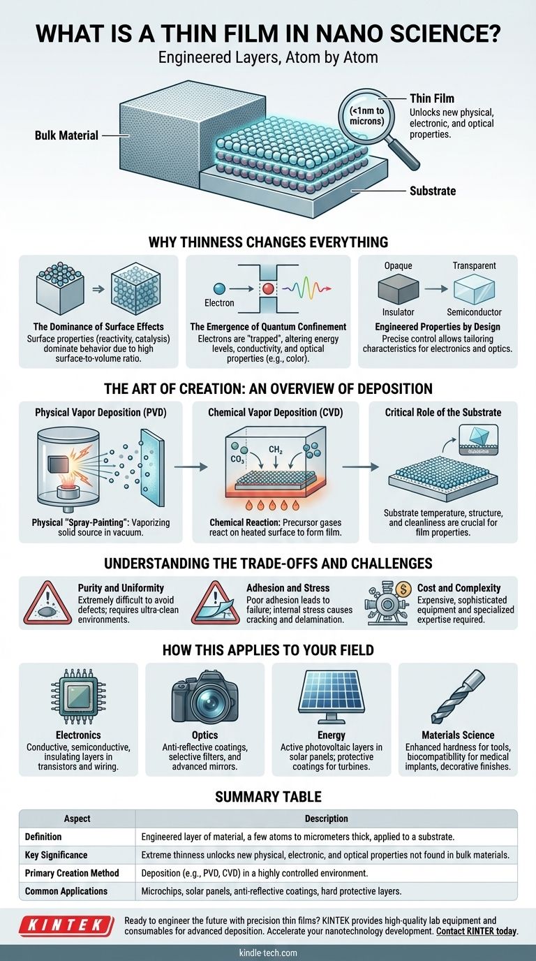
In the realm of nanoscience, a thin film is an engineered layer of material, often just a few atoms thick, that is precisely applied to a surface. These films range in thickness from a single atomic layer (less than a nanometer) to several micrometers. They are created through a highly controlled process called deposition, where a material is transformed into a vapor or plasma and then allowed to condense onto a target object, known as a substrate.
The true significance of a thin film is not merely its minimal thickness. It is how this extreme confinement unlocks new physical, electronic, and optical properties that the material does not possess in its bulk form, enabling the construction of advanced technology from the atom up.
Why Thinness Changes Everything
The properties of a material are not static; they change dramatically when one or more of its dimensions are shrunk to the nanoscale. A thin film is fundamentally different from a solid block of the same exact substance.
The Dominance of Surface Effects
In a large, bulk material, most atoms are surrounded by other atoms. In a thin film, a massive proportion of the atoms are on the surface or near an interface. This makes surface properties, such as chemical reactivity and catalytic activity, the dominant factors governing the film's behavior.
The Emergence of Quantum Confinement
When a material becomes thin enough (typically below 50 nanometers), electrons are "trapped" or confined in one dimension. This quantum mechanical effect fundamentally alters their available energy levels. Just as a shorter guitar string produces a higher note, this confinement changes how the material interacts with electricity and light, altering its conductivity and color.
Engineered Properties by Design
By precisely controlling a film's thickness, crystal structure, and composition, we can engineer its properties. A material that is opaque in bulk can become transparent as a thin film. An insulator can become a semiconductor. This ability to tailor material characteristics is the cornerstone of modern electronics and optics.
The Art of Creation: An Overview of Deposition
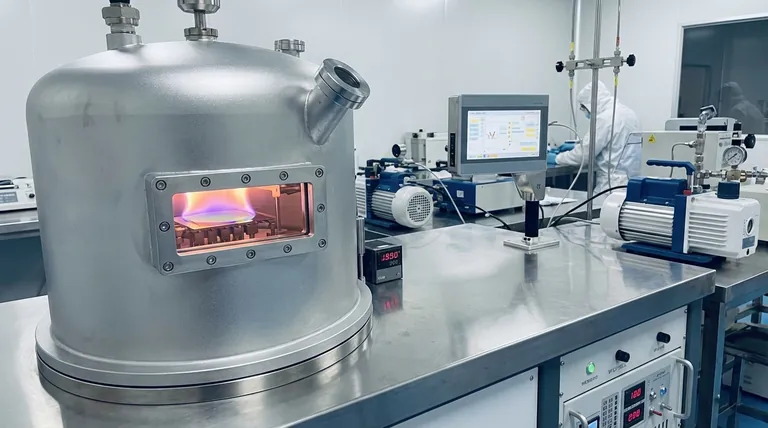
Thin films are not simply sliced from a larger block; they are built atom-by-atom or molecule-by-molecule on a substrate. This process is called deposition and generally falls into two major categories.
Physical Vapor Deposition (PVD)
PVD is a "physical" process, akin to a form of molecular spray-painting inside a high-vacuum chamber. A solid source material is bombarded with energy, causing it to vaporize into individual atoms or molecules. This vapor then travels through the vacuum and condenses onto the cooler substrate, forming a thin, uniform film.
Chemical Vapor Deposition (CVD)
CVD is a "chemical" process where precursor gases are introduced into a reaction chamber. These gases react or decompose on the surface of a heated substrate, leaving behind a solid material to form the film. It is a method for building highly pure, crystalline films one molecular layer at a time.
The Critical Role of the Substrate
The thin film is always deposited onto something, like a silicon wafer, glass, or metal. The substrate is not just a passive holder; its temperature, crystal structure, and surface cleanliness are critical factors that influence the final properties of the film itself.
Understanding the Trade-offs and Challenges
While thin films are enabling, their creation and use come with significant technical hurdles that define the limits of the technology.
The Challenge of Purity and Uniformity
Creating a perfect film is exceptionally difficult. A single stray dust particle or an unwanted atom of gas inside the deposition chamber can create a defect that ruins an entire microelectronic device. Achieving a perfectly even thickness across a large surface like a silicon wafer requires incredibly sophisticated equipment.
The Problem of Adhesion and Stress
A film is only useful if it sticks firmly to its substrate. Poor adhesion can cause the film to peel or flake off. Furthermore, immense internal stress can build up in the film during the deposition process, causing it to crack and fail, sometimes long after it has been manufactured.
The Barrier of Cost and Complexity
The equipment required for high-quality thin film deposition—including high-vacuum chambers, ultra-pure source materials, and precise control systems—is extremely expensive to acquire and operate. It demands a cleanroom environment and highly specialized expertise, placing it far beyond the reach of casual experimentation.
How This Applies to Your Field
The application of thin films is not an abstract scientific concept; it is the invisible foundation of the modern world. Understanding their purpose allows you to recognize their role in nearly every piece of advanced technology.
- If your primary focus is electronics: You will rely on thin films as the conductive, semiconductive, and insulating layers that form the transistors and wiring inside microchips.
- If your primary focus is optics: You will use thin films to create anti-reflective coatings on glasses and camera lenses, or as the selective layers in advanced optical filters and mirrors.
- If your primary focus is energy: You will see thin films as the active photovoltaic layers in solar panels or as ultra-hard, corrosion-resistant coatings that protect turbine blades.
- If your primary focus is materials science: You will study thin films to develop materials with enhanced hardness for tools, improved biocompatibility for medical implants, or unique decorative finishes.
Ultimately, to understand thin films is to understand the fundamental building blocks of modern device engineering.
Summary Table:
| Aspect | Description |
|---|---|
| Definition | An engineered layer of material, a few atoms to micrometers thick, applied to a substrate. |
| Key Significance | Extreme thinness unlocks new physical, electronic, and optical properties not found in bulk materials. |
| Primary Creation Method | Deposition (e.g., PVD, CVD) in a highly controlled environment. |
| Common Applications | Microchips, solar panels, anti-reflective coatings, hard protective layers. |
Ready to engineer the future with precision thin films?
KINTEK specializes in providing the high-quality lab equipment and consumables essential for advanced thin film deposition. Whether your focus is on electronics, optics, energy, or materials science, our solutions support the creation of superior, defect-free films. From research to production, we help you achieve the purity, uniformity, and adhesion your projects demand.
Contact KINTEK today to discuss how our expertise can accelerate your nanotechnology development.
Visual Guide
Related Products
- Aluminum-Plastic Flexible Packaging Film for Lithium Battery Packaging
- Thin-Layer Spectral Electrolysis Electrochemical Cell
People Also Ask
- How is aluminum foil utilized as a consumable during the assembly of cold sintering molds? Optimize Tooling Longevity
- What is the thinnest coating? Unlocking Unique Properties at the Atomic Scale
- How to tell if a lithium-ion battery is bad? Spot the critical signs of failure before it's too late.
- What is the difference between single layer film and multi layer film? A Guide to Material Selection
- Is there a way to test lithium batteries? Understand Voltage vs. True Health

