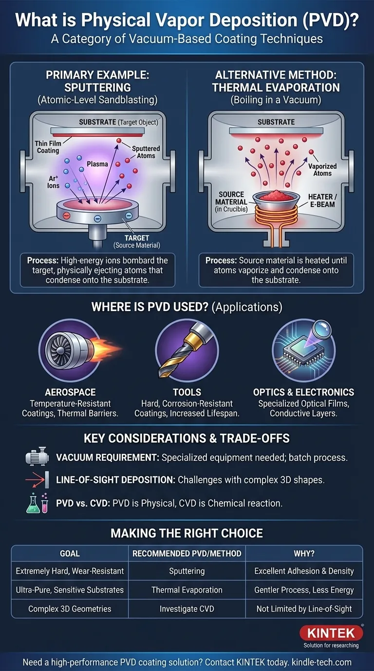
A primary example of physical vapor deposition (PVD) is sputtering. This process involves bombarding a solid source material, known as the target, with high-energy ions inside a vacuum. This atomic-level collision physically ejects or "sputters" atoms from the target, which then travel through the vacuum and condense onto a substrate to form an extremely thin, high-performance coating.
Physical vapor deposition is not a single process, but a category of vacuum-based coating techniques. The core principle involves physically transforming a solid material into a vapor, which then condenses atom-by-atom onto a surface to create a durable thin film.
How Do PVD Processes Work?
To understand PVD, it's essential to grasp the fundamental mechanism and the most common methods used to achieve it.
The Core Principle: Solid to Vapor to Solid
All PVD processes operate inside a vacuum chamber. This is critical because it removes air and other particles that could react with or impede the vaporized material.
The process involves two key stages. First, a high-energy source is used to convert a solid source material into a vapor. Second, this vapor travels through the vacuum and condenses onto the target object (the substrate), forming a thin, uniform film.
Example 1: Sputtering
Sputtering can be thought of as atomic-level sandblasting. In this method, a high voltage is applied, and inert gas (like argon) is introduced into the vacuum chamber.
This creates plasma, and the positively charged gas ions accelerate and strike the negatively charged source material (the target). The impact has enough energy to knock individual atoms off the target's surface, which then deposit onto the substrate.
Example 2: Thermal Evaporation
Thermal evaporation is another major PVD technique. This process works more like boiling a liquid, but with solid materials in a vacuum.
The source material is heated using methods like resistance heating or a high-energy electron beam (e-beam evaporation) until its atoms vaporize. These vaporized atoms then travel through the vacuum and condense on the cooler substrate, creating the thin film.
Where is PVD Actually Used?
The unique properties of PVD coatings make them indispensable in several high-tech industries. The applications are a direct result of the process's ability to create extremely thin yet highly durable films.
Aerospace and High-Temperature Components
Aerospace companies use PVD, particularly e-beam evaporation, to apply dense, temperature-resistant coatings to engine parts. These films act as thermal barriers, allowing components to withstand extreme temperatures and enhancing overall durability.
Protective Coatings for Tools
PVD is widely used to apply hard, corrosion-resistant coatings to cutting tools, drills, and industrial molds. These coatings, often just a few microns thick, dramatically increase the lifespan and performance of tools used in harsh environments.
Advanced Optics and Electronics
The technique is also critical for applying specialized optical films for solar panels and anti-reflective coatings on lenses. In the semiconductor industry, PVD is used to deposit the thin layers of conductive and insulating materials that form the basis of microchips.
Understanding the Trade-offs and Key Considerations
While powerful, PVD is not a universal solution. Understanding its operational requirements is key to deciding if it's the right process for a given application.
The Vacuum Requirement
The need for a high-vacuum environment means that PVD requires specialized, and often expensive, equipment. The process is typically performed in batches, which can be slower than continuous, atmospheric-pressure coating methods.
Line-of-Sight Deposition
Most PVD processes are "line-of-sight," meaning the vaporized material travels in a straight line from the source to the substrate. This makes it challenging to uniformly coat complex, three-dimensional shapes or the inside of cavities without sophisticated rotating fixtures for the substrate.
Distinguishing PVD from CVD
It's common to confuse PVD with Chemical Vapor Deposition (CVD). The key difference is simple: PVD is a physical process (evaporating, bombarding). In contrast, CVD uses a chemical reaction where precursor gases react on a heated substrate to form the solid film.
Making the Right Choice for Your Goal
Selecting the correct deposition technique depends entirely on the desired properties of the final coating and the nature of the substrate.
- If your primary focus is creating extremely hard, wear-resistant coatings: Sputtering is often preferred for its excellent film adhesion and density.
- If your primary focus is depositing ultra-pure films on sensitive substrates (like optics or electronics): Thermal evaporation is often a better choice because it's a gentler process that imparts less energy to the substrate.
- If your primary focus is coating complex 3D geometries uniformly: You may need to investigate alternatives like Chemical Vapor Deposition (CVD), which is not limited by line-of-sight deposition.
Understanding these fundamental PVD methods empowers you to select the precise surface engineering solution for your application.
Summary Table:
| PVD Process | Key Mechanism | Common Applications |
|---|---|---|
| Sputtering | Bombards target with ions to eject atoms | Hard coatings for tools, semiconductor films |
| Thermal Evaporation | Heats material to vaporize atoms | Optical coatings, pure films for electronics |
Need a high-performance PVD coating solution for your lab or production? KINTEK specializes in lab equipment and consumables, providing expert guidance on sputtering, thermal evaporation, and other PVD techniques to enhance durability, performance, and efficiency. Contact us today to discuss your specific application and achieve superior results!
Visual Guide
Related Products
- Chemical Vapor Deposition CVD Equipment System Chamber Slide PECVD Tube Furnace with Liquid Gasifier PECVD Machine
- RF PECVD System Radio Frequency Plasma-Enhanced Chemical Vapor Deposition RF PECVD
- 915MHz MPCVD Diamond Machine Microwave Plasma Chemical Vapor Deposition System Reactor
- HFCVD Machine System Equipment for Drawing Die Nano-Diamond Coating
- Customer Made Versatile CVD Tube Furnace Chemical Vapor Deposition Chamber System Equipment
People Also Ask
- How expensive is chemical vapor deposition? Understanding the True Cost of High-Performance Coating
- What types of substrates are used in CVD to facilitate graphene films? Optimize Graphene Growth with the Right Catalyst
- How are carbon nanotubes grown? Master Scalable Production with Chemical Vapor Deposition
- What happens during deposition chemistry? Building Thin Films from Gaseous Precursors
- What are the advantages of chemical vapor deposition? Achieve Superior Thin Films for Your Lab


