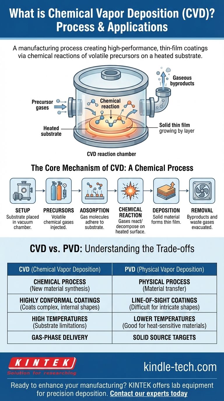
In short, Chemical Vapor Deposition (CVD) is a manufacturing process that creates a high-performance, thin-film coating on a substrate. It works by introducing volatile chemical gases, known as precursors, into a reaction chamber. These gases then react or decompose on a heated surface, forming a solid material that deposits evenly onto the target object, building the coating one layer of molecules at a time.
The core principle to understand is that CVD is fundamentally a chemical process, not a physical one. Unlike methods that simply move a material from a source to a target, CVD synthesizes an entirely new solid material directly on the component's surface through controlled chemical reactions.
The Core Mechanism of CVD
To truly grasp the CVD process, it's best to break it down into its sequential steps. The entire operation takes place within a sealed reaction chamber under carefully controlled temperature, pressure, and vacuum conditions.
The Setup: Chamber and Precursors
The process begins by placing the object to be coated, known as the substrate, inside a reaction chamber. The chamber is then evacuated to create a vacuum. Special volatile chemical compounds, called precursors, are selected based on the desired final coating material.
Step 1: Introducing the Precursors
The precursor chemicals, which are in a gaseous state, are precisely injected into the vacuum chamber. The flow rate and mixture of these gases are critical variables that control the final properties of the coating.
Step 2: Transport and Adsorption
Once inside the chamber, the precursor gas molecules travel and come into contact with the substrate. The molecules then physically stick to the surface in a process known as adsorption.
Step 3: The Chemical Reaction
This is the heart of the CVD process. The substrate is typically heated to a specific reaction temperature. This thermal energy provides the activation energy needed for the adsorbed precursor gases to react with each other or decompose directly on the surface.
Step 4: Deposition and Film Growth
The product of this chemical reaction is the desired solid coating material. This nonvolatile solid deposits onto the substrate, forming a stable, thin film. The process continues as more gas is supplied, allowing the film to grow in a highly uniform and controlled manner.
Step 5: Removing the Byproducts
The chemical reactions also create gaseous byproducts that are not part of the final coating. These waste gases are desorbed from the surface and are continuously removed from the chamber by the vacuum system, ensuring a pure and high-quality film.
Understanding the Trade-offs: CVD vs. PVD
To understand the specific advantages of CVD, it is helpful to contrast it with another common thin-film deposition technique: Physical Vapor Deposition (PVD).
The Fundamental Difference: Chemical vs. Physical
The primary distinction is in the name. CVD uses a chemical reaction on the substrate's surface to create the coating. In contrast, PVD uses a physical mechanism—such as evaporation or sputtering—to move atoms of the coating material from a solid source directly onto the substrate. There is no chemical transformation in PVD.
Coating Characteristics
Because CVD relies on a gas that can flow and permeate, it excels at creating highly conformal coatings, meaning it can uniformly cover complex shapes, sharp corners, and even internal surfaces. PVD is typically a "line-of-sight" process, which can make it difficult to coat intricate geometries evenly.
Process Conditions
CVD processes generally require high temperatures to provide the energy needed to drive the chemical reactions. This can limit the types of substrate materials that can be coated without being damaged. PVD can often be performed at much lower temperatures, making it suitable for more heat-sensitive materials.
Making the Right Choice for Your Goal
Selecting the correct deposition method depends entirely on the specific requirements of your application, including the material properties, substrate shape, and temperature constraints.
- If your primary focus is a high-purity, uniform coating on a complex shape: CVD is an exceptionally strong candidate due to the nature of its gas-phase delivery.
- If your primary focus is coating a temperature-sensitive material: PVD is often the better choice because it can be operated at significantly lower process temperatures than most CVD methods.
- If your primary focus is a specific material composition: The choice depends on the availability of suitable volatile precursors for CVD versus solid targets for PVD for that particular material.
Ultimately, understanding CVD as a precision chemical reaction process is the key to leveraging its unique capabilities for advanced material fabrication.
Summary Table:
| CVD Process Step | Key Action | Outcome |
|---|---|---|
| 1. Setup | Substrate placed in vacuum chamber | Prepares surface for coating |
| 2. Gas Introduction | Precursor gases injected into chamber | Delivers coating materials |
| 3. Adsorption | Gas molecules stick to substrate surface | Creates foundation for reaction |
| 4. Chemical Reaction | Gases react/decompose on heated surface | Forms solid coating material |
| 5. Deposition | Solid material builds up layer by layer | Creates uniform thin film |
| 6. Byproduct Removal | Waste gases evacuated from chamber | Ensures coating purity |
Ready to enhance your manufacturing with precision coatings? KINTEK specializes in lab equipment and consumables for advanced deposition processes like CVD. Our solutions help laboratories achieve superior thin-film results with high uniformity and purity. Contact our experts today to discuss how we can support your specific application needs!
Visual Guide
Related Products
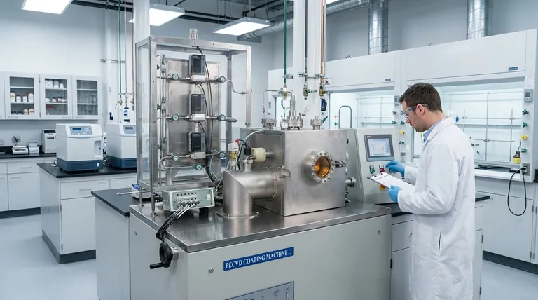
- Chemical Vapor Deposition CVD Equipment System Chamber Slide PECVD Tube Furnace with Liquid Gasifier PECVD Machine
- RF PECVD System Radio Frequency Plasma-Enhanced Chemical Vapor Deposition RF PECVD
- Microwave Plasma Chemical Vapor Deposition MPCVD Machine System Reactor for Lab and Diamond Growth
- Customer Made Versatile CVD Tube Furnace Chemical Vapor Deposition Chamber System Equipment
- 915MHz MPCVD Diamond Machine Microwave Plasma Chemical Vapor Deposition System Reactor
People Also Ask
- Why is Chemical Vapor Deposition (CVD) equipment uniquely suited for constructing hierarchical superhydrophobic structures?
- What are the core advantages of PE-CVD in OLED encapsulation? Protect Sensitive Layers with Low-Temp Film Deposition
- What is plasma enhanced chemical vapor deposition PECVD equipment? A Guide to Low-Temperature Thin Film Deposition
- What types of substrates are used in CVD to facilitate graphene films? Optimize Graphene Growth with the Right Catalyst
- How expensive is chemical vapor deposition? Understanding the True Cost of High-Performance Coating


