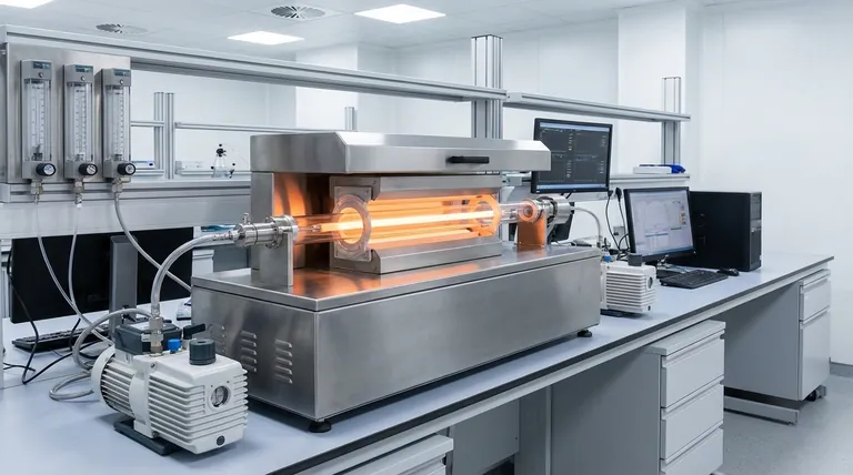
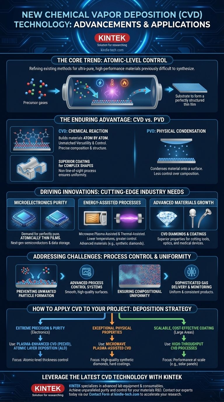
In the field of material science, "new" Chemical Vapor Deposition (CVD) technology is not a single invention, but rather a series of critical advancements in process control and energy sources. These enhancements, such as microwave plasma-assisted and thermal-assisted techniques, are designed to create materials of unprecedented purity and performance. This evolution is driven by the relentless demands of high-growth sectors like microelectronics and advanced materials, such as synthetic diamonds.
The core trend in modern CVD is the refinement of existing methods to gain atomic-level control over material creation. This allows for the production of ultra-pure, high-performance thin films and materials that were previously difficult or impossible to synthesize efficiently.
The Enduring Advantage of CVD
Chemical Vapor Deposition is a process where a thin solid film is grown on a substrate through chemical reactions involving vapor-phase precursors. Unlike Physical Vapor Deposition (PVD), which essentially condenses a material onto a surface, CVD builds materials atom by atom through chemistry.
Unmatched Versatility and Control
The foundation of CVD's power lies in its reliance on chemical reactions. This gives engineers and scientists precise control over the composition and structure of the final material.
By carefully managing precursor gases, temperature, and pressure, it's possible to create ultra-thin layers of material with exceptional purity. This is fundamental to the production of modern electrical circuits.
Superior Coating for Complex Shapes
CVD is a non-line-of-sight process. The precursor gases can flow around and into complex geometries, ensuring a uniform and even coating on all surfaces.
This makes it ideal for components with intricate shapes, providing a consistent layer that other deposition methods struggle to achieve.
What's Driving the Latest Innovations?
The evolution of CVD is directly tied to the needs of cutting-edge industries. Modern advancements are focused on overcoming historical limitations and unlocking new material capabilities.
The Demand for Purity in Microelectronics
The microelectronics industry remains the largest user of CVD technology. The continuous shrinking of transistors requires the deposition of perfectly pure, defect-free, and atomically thin films.
Newer CVD techniques provide the enhanced thickness control and material purity necessary to build the next generation of semiconductors and data storage devices.
Advancements in Energy-Assisted Processes
Techniques like microwave plasma-assisted CVD and thermal-assisted CVD represent a significant leap forward. These methods use energy to activate the precursor gases more efficiently.
This allows deposition to occur at lower temperatures and with greater control, enabling the creation of advanced materials, like high-quality synthetic diamonds, with exceptional hardness, thermal conductivity, and optical properties.
The Growth of Advanced Materials
The cost-effectiveness and superior properties of materials like CVD diamonds have opened up new markets. They are now used in cutting tools, optics, and even medical equipment.
These applications are possible because advanced CVD processes can produce materials that outperform their natural or conventionally made counterparts.
Understanding the Trade-offs and Challenges
While powerful, CVD technology is not without its challenges. The very innovations in the field are aimed at mitigating these inherent complexities.
Preventing Unwanted Particle Formation
One of the primary challenges is the formation of hard aggregates in the gas phase before the material can deposit on the substrate. This can lead to defects in the final film.
Advanced process control systems and reactor designs are crucial for minimizing this effect and ensuring a smooth, high-quality surface.
Ensuring Compositional Uniformity
When creating multi-component materials (alloys or compounds), variations in vapor pressure and reaction rates can lead to a heterogeneous composition.
The latest CVD systems employ sophisticated gas delivery and monitoring to ensure each precursor reacts at the correct rate, resulting in a uniform and consistent final product.
How to Apply This to Your Project
The best deposition strategy depends entirely on your primary goal. CVD offers a range of possibilities tailored to specific outcomes.
- If your primary focus is extreme precision and purity for electronics: You will need advanced CVD processes like Plasma-Enhanced CVD (PECVD) or Atomic Layer Deposition (a subset of CVD) for their atomic-level thickness control.
- If your primary focus is creating materials with exceptional physical properties: Look into specialized techniques like microwave plasma-assisted CVD, which is essential for producing high-quality synthetic diamonds and other hard coatings.
- If your primary focus is scalable, cost-effective coating for large areas like solar panels: A high-throughput, well-established CVD process is likely the most economical and efficient choice for achieving good performance at scale.
Ultimately, the ongoing innovation in Chemical Vapor Deposition is about mastering chemistry to build the foundational materials of future technology.
Summary Table:
| Aspect of Innovation | Key Advancement | Primary Benefit |
|---|---|---|
| Process Control | Atomic-level precision | Ultra-pure, defect-free thin films |
| Energy Source | Plasma & Thermal Assistance | Lower temperature deposition, new materials (e.g., diamonds) |
| Application Focus | Microelectronics & Advanced Materials | Superior performance for semiconductors, cutting tools, optics |
| Key Challenge Addressed | Minimized particle formation & enhanced uniformity | High-quality, consistent coatings on complex shapes |
Ready to leverage the latest CVD technology for your materials project?
KINTEK specializes in advanced lab equipment and consumables, providing the precise tools needed for plasma-assisted CVD, thermal-assisted CVD, and other cutting-edge deposition processes. Whether you are developing next-generation semiconductors, synthetic diamonds, or high-performance coatings, our solutions are designed to help you achieve unparalleled purity and control.
Contact our experts today via our Contact Form to discuss how our CVD solutions can accelerate your research and development.
Visual Guide
Related Products
- Chemical Vapor Deposition CVD Equipment System Chamber Slide PECVD Tube Furnace with Liquid Gasifier PECVD Machine
- Microwave Plasma Chemical Vapor Deposition MPCVD Machine System Reactor for Lab and Diamond Growth
- 915MHz MPCVD Diamond Machine Microwave Plasma Chemical Vapor Deposition System Reactor
- Customer Made Versatile CVD Tube Furnace Chemical Vapor Deposition Chamber System Equipment
- Split Chamber CVD Tube Furnace with Vacuum Station Chemical Vapor Deposition System Equipment Machine
People Also Ask
- What is the chemical vapor deposition growth process? Build Superior Thin Films from the Atom Up
- Why is Chemical Vapor Deposition (CVD) equipment uniquely suited for constructing hierarchical superhydrophobic structures?
- What are the processes of vapor phase deposition? Understand CVD vs. PVD for Superior Thin Films
- How are carbon nanotubes grown? Master Scalable Production with Chemical Vapor Deposition
- What are the core advantages of PE-CVD in OLED encapsulation? Protect Sensitive Layers with Low-Temp Film Deposition


