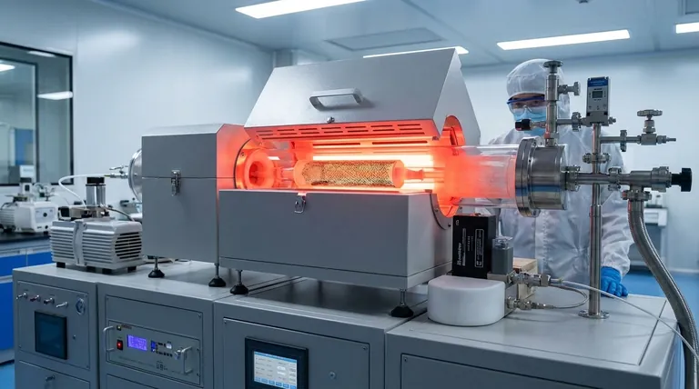
In essence, chemical vapor deposition (CVD) is a synthesis process where a material is built up from a gas phase onto a solid surface. Precursor gases containing the desired chemical elements are introduced into a reaction chamber, where they decompose and react at high temperatures, depositing a high-quality solid film or nanostructure onto a target substrate. This method is prized for its precision and ability to create materials like graphene and carbon nanotubes with superior purity and structural integrity.
CVD is not merely a coating technique; it is a "bottom-up" fabrication method that grants scientists precise, atom-by-atom control over a material's properties. By carefully managing gases, temperature, and pressure, it enables the creation of advanced nanomaterials that are often impossible to produce with conventional methods.
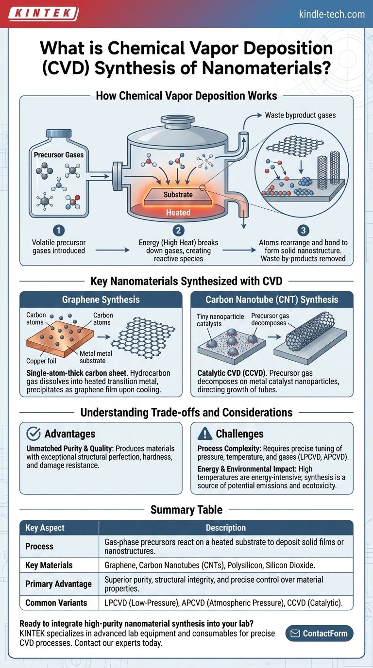
How Chemical Vapor Deposition Works
The CVD process transforms gaseous molecules into solid nanomaterials through a carefully controlled sequence of events.
The Core Mechanism
The foundation of CVD is a chemical reaction on a heated surface. Volatile precursor gases, which contain the atoms needed for the final material, are passed over a substrate inside a reaction chamber.
The Role of Energy
Energy, typically in the form of high heat, is applied to the substrate. This energy breaks down the precursor gases into reactive species that then adsorb onto the substrate surface.
Building the Nanostructure
Once on the surface, these atoms rearrange themselves and bond together, forming a stable, solid thin film or discrete nanostructures. The waste by-products of the reaction are then pumped out of the chamber, leaving only the desired material behind.
Key Nanomaterials Synthesized with CVD
CVD's versatility makes it the preferred method for producing some of the most critical nanomaterials used in modern technology.
Graphene Synthesis
To create graphene, a single-atom-thick sheet of carbon, a hydrocarbon gas is typically introduced into a chamber with a transition metal substrate, like copper or nickel.
At very high temperatures, carbon atoms from the gas dissolve into the metal. As the substrate cools, the carbon's solubility in the metal decreases, causing the carbon atoms to precipitate out and form a continuous graphene film on the surface.
Carbon Nanotube (CNT) Synthesis
The most common method for producing CNTs is Catalytic CVD (CCVD). This process uses tiny nanoparticles of a catalyst metal (like iron or cobalt) to direct the growth of the tubes.
The precursor carbon gas decomposes exclusively on the surface of these catalyst particles, from which the nanotube then grows. This technique offers excellent control over the resulting CNTs' structure and is highly cost-effective.
Other Advanced Films
Beyond carbon nanomaterials, CVD is essential for producing other high-purity films. Polysilicon, a key material in the solar photovoltaic industry, and silicon dioxide, a fundamental component in microelectronics, are both commonly produced using variations of CVD.
Understanding the Trade-offs and Considerations
While powerful, CVD is not a universal solution. Understanding its advantages and limitations is crucial for proper application.
Advantage: Unmatched Purity and Quality
The primary benefit of CVD is its ability to produce materials with exceptionally high purity and structural perfection. The resulting films are often harder and more resistant to damage compared to those made with other methods.
Challenge: Process Complexity
CVD is not a single technique but a family of processes, including Low-Pressure CVD (LPCVD) and Atmospheric Pressure CVD (APCVD). The choice of pressure, temperature, and precursor gases must be precisely tuned for the specific material, making the process complex to optimize.
Challenge: Energy and Environmental Impact
CVD processes often require very high temperatures, making them energy-intensive. The synthesis process itself—including material consumption and energy use—is a significant source of potential environmental impact, including greenhouse gas emissions and ecotoxicity.
Making the Right Choice for Your Goal
Selecting the appropriate CVD parameters is critical and depends entirely on your end goal.
- If your primary focus is ultimate material purity for advanced electronics: You will need a highly controlled process like Low-Pressure (LPCVD) or Ultra-High Vacuum CVD (UHVCVD), which justifies the higher equipment cost.
- If your primary focus is high-volume, cost-effective production for solar cells or coatings: A simpler method like Atmospheric Pressure CVD (APCVD) or a well-optimized Catalytic CVD (CCVD) process is often the most suitable approach.
- If your primary focus is sustainability and minimizing environmental impact: You must prioritize optimizing for lower energy consumption and selecting precursor materials and catalysts with lower lifecycle ecotoxicity.
Ultimately, mastering CVD is a balancing act between achieving ideal material properties, production scalability, and environmental responsibility.
Summary Table:
| Key Aspect | Description |
|---|---|
| Process | Gas-phase precursors react on a heated substrate to deposit solid films or nanostructures. |
| Key Materials | Graphene, Carbon Nanotubes (CNTs), Polysilicon, Silicon Dioxide. |
| Primary Advantage | Superior purity, structural integrity, and precise control over material properties. |
| Common Variants | LPCVD (Low-Pressure), APCVD (Atmospheric Pressure), CCVD (Catalytic). |
Ready to integrate high-purity nanomaterial synthesis into your lab? KINTEK specializes in advanced lab equipment and consumables for precise CVD processes. Our expertise helps laboratories achieve superior material quality and research outcomes. Contact our experts today to discuss your specific needs and how we can support your innovative work.
Visual Guide
Related Products
- Cylindrical Resonator MPCVD Machine System Reactor for Microwave Plasma Chemical Vapor Deposition and Lab Diamond Growth
- HFCVD Machine System Equipment for Drawing Die Nano-Diamond Coating
- Microwave Plasma Chemical Vapor Deposition MPCVD Machine System Reactor for Lab and Diamond Growth
- Customer Made Versatile CVD Tube Furnace Chemical Vapor Deposition Chamber System Equipment
- 915MHz MPCVD Diamond Machine Microwave Plasma Chemical Vapor Deposition System Reactor
People Also Ask
- How does a microwave plasma reactor facilitate the synthesis of diamond? Master MPCVD with Precision Technology
- What are the primary advantages of the CVD method for growing diamonds? Engineering High-Purity Gems and Components
- What are the advantages of a Microwave Plasma CVD reactor for MCD/NCD coatings? Precision Multilayer Diamond Engineering
- How does chemical vapor deposition work for diamonds? Grow Lab-Created Diamonds Layer by Layer
- What is the difference between MPCVD and HFCVD? Choose the Right CVD Method for Your Application