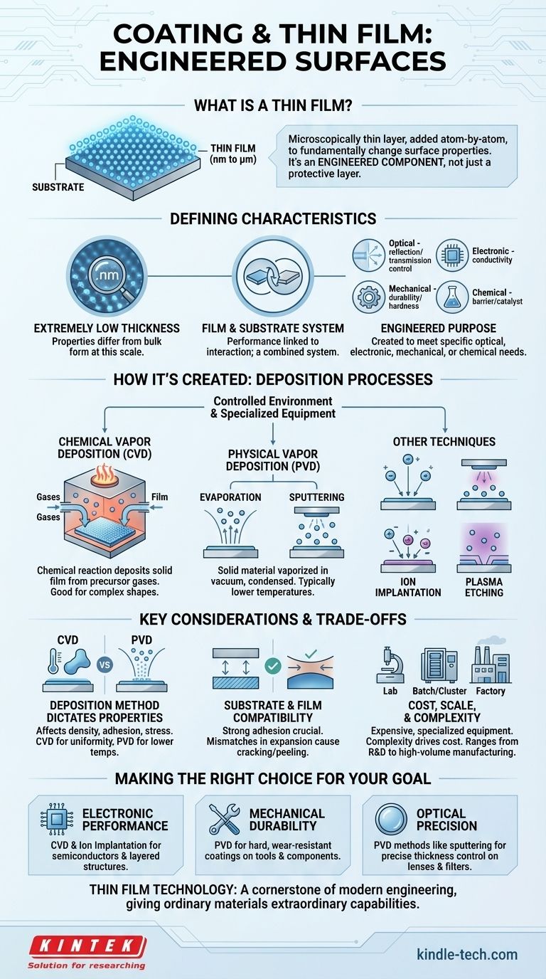
At its core, a thin film coating is a microscopically thin layer of material, ranging from fractions of a nanometer to several micrometers thick, that is applied to a surface. This process, known as deposition, is not like painting; it involves carefully adding material atom-by-atom to fundamentally change the surface's properties, such as making it scratch-resistant, electrically conductive, or optically reflective.
The critical concept to grasp is that a thin film isn't just a protective layer. It is an engineered component that grants a base material (the substrate) entirely new and specific functionalities that it doesn't possess on its own.
What Defines a Thin Film?
A simple layer of paint is a coating, but it is not a "thin film" in the technical sense. The distinction lies in the precision of the application, the microscopic thickness, and the specific function it is designed to perform.
More Than Just a Layer
The defining characteristic of a thin film is its extremely low thickness. At this scale, the material's properties can differ significantly from its bulk form. This precision allows for the manipulation of light, electricity, and durability in ways that a thicker coating cannot achieve.
The Film and Substrate as a System
A thin film does not exist in isolation. Its performance is fundamentally linked to the surface it is applied to, known as the substrate. The final characteristics of the coated product are a result of the interaction between the film's material, its thickness, and the underlying properties of the substrate itself.
Engineered for a Specific Purpose
Thin films are created to meet highly specific requirements. These goals can be broadly categorized, and often a single film must satisfy needs across multiple categories.
- Optical: Controlling the reflection or transmission of light, used in eyeglass coatings, camera lenses, and solar cells.
- Electronic: Increasing or decreasing electrical conductivity, essential for semiconductors, microchips, and display screens.
- Mechanical: Enhancing durability, hardness, and resistance to scratches or corrosion, used on cutting tools and engine parts.
- Chemical: Creating a barrier to prevent reactions or providing a catalytic surface.
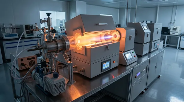
How Thin Films Are Created: The Deposition Process
Applying these microscopic layers requires highly controlled environments and specialized equipment. The goal is to produce a film with excellent homogeneity (uniformity) and low surface roughness.
Chemical Vapor Deposition (CVD)
In CVD, the substrate is placed in a chamber filled with one or more precursor gases. An energy source (like heat or plasma) is introduced, causing a chemical reaction that deposits a solid film onto the substrate's surface.
Physical Vapor Deposition (PVD)
PVD encompasses methods where a solid material is vaporized in a vacuum and then condensed onto the substrate. The two most common forms are evaporation, where the material is heated until it evaporates, and sputtering, where a target is bombarded with high-energy ions, knocking atoms loose that then deposit on the substrate.
Other Surface Modification Techniques
Other related processes modify the surface at an atomic level. Ion implantation directs charged atoms at a surface to alter its properties, while plasma etching uses plasma to precisely remove material layers, often in the manufacturing of integrated circuits.
Understanding the Trade-offs and Key Considerations
The decision to use a particular thin film technology is not arbitrary. It involves a careful balance of performance requirements, material compatibility, and cost.
Deposition Method Dictates Properties
The choice between CVD and PVD, for example, has significant consequences. CVD can often coat complex shapes more uniformly, while PVD processes are typically run at lower temperatures, making them suitable for substrates that cannot withstand high heat. Each method imparts different levels of density, adhesion, and internal stress to the film.
Substrate and Film Compatibility
A successful coating requires strong adhesion to the substrate. Mismatches in properties, such as how much the materials expand or contract with temperature, can cause the film to crack or peel away. The substrate's cleanliness and surface texture are also critical for a successful application.
Cost, Scale, and Complexity
The equipment for thin film deposition is highly specialized and expensive.
- Laboratory systems are small and used for research and development.
- Batch and cluster systems process multiple components at once for medium-scale production.
- Factory systems are large, often automated, and designed for high-volume manufacturing.
The complexity of the process and the required equipment are major factors in the final cost of the coated product.
Making the Right Choice for Your Goal
The optimal thin film and deposition method are entirely dependent on the intended application.
- If your primary focus is electronic performance: CVD and ion implantation are foundational processes for creating the complex, layered structures in semiconductors.
- If your primary focus is mechanical durability: PVD techniques are a top choice for applying hard, wear-resistant coatings to tools, medical implants, and industrial components.
- If your primary focus is optical precision: PVD methods like sputtering provide exceptional control over film thickness, which is critical for anti-reflection coatings on lenses and filters.
Thin film technology is a cornerstone of modern engineering, enabling us to give ordinary materials extraordinary capabilities.
Summary Table:
| Key Aspect | Description |
|---|---|
| Thickness | Nanometers to micrometers; alters material properties at a microscopic scale. |
| Function | Engineered for optical, electronic, mechanical, or chemical performance. |
| Deposition Methods | Chemical Vapor Deposition (CVD) and Physical Vapor Deposition (PVD). |
| Substrate Compatibility | Critical for adhesion; depends on material properties and surface preparation. |
Ready to enhance your materials with precision thin film coatings? KINTEK specializes in advanced lab equipment and consumables for CVD, PVD, and surface modification processes. Whether you're developing semiconductors, durable tools, or optical components, our solutions deliver the uniformity, adhesion, and performance your R&D or production demands. Contact our experts today to discuss how we can support your laboratory's coating challenges.
Visual Guide
Related Products
- HFCVD Machine System Equipment for Drawing Die Nano-Diamond Coating
- Chemical Vapor Deposition CVD Equipment System Chamber Slide PECVD Tube Furnace with Liquid Gasifier PECVD Machine
- Customer Made Versatile CVD Tube Furnace Chemical Vapor Deposition Chamber System Equipment
- Custom CVD Diamond Coating for Lab Applications
- 915MHz MPCVD Diamond Machine Microwave Plasma Chemical Vapor Deposition System Reactor
People Also Ask
- What are the disadvantages and challenges of the HFCVD method? Overcome Growth Limits and Filament Issues
- What is the hot filament chemical vapour deposition of diamond? A Guide to Synthetic Diamond Coating
- What are the advantages of chemical vapor deposition? Achieve Superior Thin Films for Your Lab
- What is the function of tungsten filaments in HFCVD? Powering Diamond Film Synthesis with Thermal Excitation
- What is the full form of HFCVD? A Guide to Hot Filament Chemical Vapor Deposition


