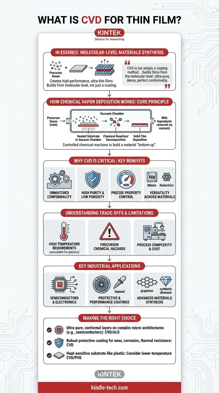
In essence, Chemical Vapor Deposition (CVD) is a highly versatile manufacturing process used to create extremely thin, high-performance films on a substrate's surface. It works by introducing precursor gases into a reaction chamber, where they decompose and react on the substrate to form a solid material, one atomic layer at a time. This method is fundamental to manufacturing advanced components, from the intricate circuitry in semiconductors to the durable coatings on medical implants.
CVD is not simply a coating method; it is a materials synthesis process that builds films from the molecular level. Its true value lies in its ability to create ultra-pure, dense, and perfectly uniform (conformal) layers that can follow the most complex surface topographies—a feat often impossible with traditional techniques.
How Chemical Vapor Deposition Works: The Core Principle
CVD is a sophisticated process that relies on controlled chemical reactions to build a material from the "bottom-up" directly onto a component's surface.
The Role of Precursor Gases
The process begins with one or more volatile precursor gases. These are chemical compounds that contain the atoms of the desired film material (e.g., silicon, carbon, titanium).
The Reaction Chamber
These gases are fed into a vacuum chamber containing the object to be coated, known as the substrate. The substrate is heated to a precise temperature, which provides the energy needed to trigger the chemical reaction.
The Deposition Process
On the hot surface of the substrate, the precursor gases react or decompose. This chemical change causes the desired atoms to "deposit" onto the surface, forming a solid, thin film. Any unwanted chemical byproducts are removed from the chamber by the vacuum system.
Why CVD is Critical for Thin Film Applications
The unique nature of the CVD process gives its films properties that are highly sought after in advanced manufacturing and technology.
Unmatched Conformality
Because the film is built molecule by molecule from a gas, it can perfectly coat every feature of a surface, including microscopic trenches, holes, and complex 3D shapes. This conformality is critical in microelectronics, where complete coverage is non-negotiable.
High Purity and Low Porosity
The controlled chemical reaction results in an exceptionally pure and dense film with very low porosity. This creates a superior barrier against corrosion, moisture, and high temperatures, protecting the underlying component.
Precise Control Over Film Properties
By carefully adjusting process parameters—such as temperature, pressure, and gas composition—engineers can precisely tune the film's thickness, electrical conductivity, hardness, and other critical properties.
Versatility Across Materials
CVD is not limited to one type of material. It is used to deposit a vast range of substances, including metals, insulating dielectrics, and advanced carbons like synthetic diamond, graphene, and carbon nanotubes.
Understanding the Trade-offs and Limitations
While powerful, CVD is not the solution for every scenario. Understanding its limitations is key to making an informed decision.
High Temperature Requirements
Many traditional CVD processes require very high temperatures to initiate the chemical reaction. This makes them unsuitable for heat-sensitive substrates, such as many plastics or biological materials, which could be damaged or destroyed.
Precursor Chemical Hazards
The precursor gases used in CVD can be highly toxic, flammable, or corrosive. This necessitates specialized handling procedures, safety monitoring, and exhaust management systems, which add to the operational complexity and cost.
Process Complexity and Cost
CVD requires sophisticated equipment, including vacuum chambers, precision gas flow controllers, and heating systems. It is generally a more complex and expensive process than simpler physical coating methods.
Specialized CVD Variants
To overcome these limitations, specialized versions of CVD have been developed. Atomic Layer Deposition (ALD), for example, is a slower, lower-temperature variant that offers unparalleled, angstrom-level control over film thickness, making it essential for next-generation electronics.
Key Industrial Applications of CVD Films
CVD's unique capabilities make it indispensable across numerous high-tech industries.
In Semiconductors and Electronics
CVD is used to create the foundational layers of microchips, including ultra-thin insulating dielectrics, conductive metal interconnects, and silicon films that form the basis of transistors.
For Protective and Performance Coatings
The process is used to apply extremely hard, wear-resistant, and thermally-resistant coatings on industrial tools and gas turbine blades. In biomedical applications, it creates biocompatible and lubricious coatings for implants.
In Advanced Materials Synthesis
CVD is a key method for producing cutting-edge materials that are difficult to make otherwise. This includes creating large, high-quality sheets of graphene, synthesizing flawless synthetic diamonds, and growing carbon nanotubes (CNTs) for use in electronics, sensors, and composites.
Making the Right Choice for Your Application
Choosing the right deposition technology depends entirely on your end goal and material constraints.
- If your primary focus is creating ultra-pure, conformal layers on complex micro-architectures (like in semiconductors): CVD or its variant, ALD, is often the only viable choice due to its atomic-level precision.
- If your primary focus is adding a robust protective coating for wear, corrosion, or thermal resistance: CVD offers a dense, non-porous film that provides superior protection compared to many mechanical or physical coating methods.
- If your primary focus is coating a heat-sensitive substrate like plastic: You must consider lower-temperature CVD variants or alternative technologies like Physical Vapor Deposition (PVD), as a traditional CVD process will likely damage the part.
Ultimately, CVD empowers engineers and scientists to design and build materials from the ground up, unlocking performance characteristics that would otherwise be unattainable.
Summary Table:
| Key Feature | Benefit |
|---|---|
| Conformal Coating | Perfectly coats complex 3D shapes and microscopic features. |
| High Purity & Density | Creates superior barrier properties against corrosion and heat. |
| Material Versatility | Deposits metals, dielectrics, diamond, graphene, and more. |
| Precise Property Control | Allows tuning of thickness, conductivity, and hardness. |
Ready to integrate CVD technology into your lab's workflow? KINTEK specializes in providing high-quality lab equipment and consumables for advanced thin-film deposition. Whether you're developing next-generation semiconductors, durable protective coatings, or synthesizing novel materials like graphene, our expertise ensures you have the right tools for precise, reliable results. Contact our experts today to discuss how we can support your laboratory's specific needs and help you achieve superior material performance.
Visual Guide
Related Products
- CVD Diamond Dressing Tools for Precision Applications
- Multi Heating Zones CVD Tube Furnace Machine Chemical Vapor Deposition Chamber System Equipment
- CVD Diamond Domes for Industrial and Scientific Applications
- CVD Diamond for Thermal Management Applications
- Chemical Vapor Deposition CVD Equipment System Chamber Slide PECVD Tube Furnace with Liquid Gasifier PECVD Machine
People Also Ask
- How long does it take to make synthetic diamonds? Discover the 6-8 Week Science Behind Lab-Grown Gems
- What is CVD diamond? The Ultimate Guide to Lab-Grown Diamonds and Their Uses
- What is chemical vapor deposition of diamond? Grow High-Purity Diamonds Atom-by-Atom
- What are the raw materials for CVD diamonds? A seed, a gas, and the science of crystal growth.
- Does the chemical vapor deposition be used for diamonds? Yes, for Growing High-Purity Lab Diamonds


