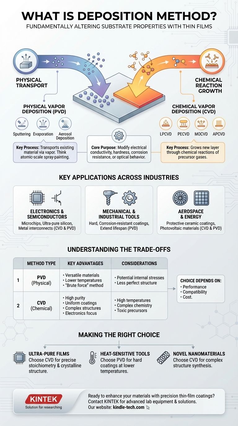
In materials science and engineering, a deposition method is any process used to apply a thin film of material onto a surface, known as a substrate. The primary purpose is to fundamentally alter the substrate's properties, such as its electrical conductivity, hardness, corrosion resistance, or optical behavior. These processes are broadly categorized into two main families: those based on physical transport and those driven by chemical reactions.
Deposition is not a single technique but a family of processes for creating high-performance coatings. The critical distinction lies in how the coating is formed: physical methods essentially "transport" an existing material onto a surface, while chemical methods "grow" a new layer through a controlled chemical reaction.
The Two Fundamental Approaches: Physical vs. Chemical
To understand deposition, you must first grasp the core difference between its two main branches: Physical Vapor Deposition (PVD) and Chemical Vapor Deposition (CVD).
Physical Deposition: The "Transport" Method
Physical deposition methods take a solid or liquid source material, turn it into a vapor, and physically transport it onto the substrate, where it condenses back into a thin solid film. Think of it as an atomic-scale spray-painting process.
This category includes techniques like sputtering, evaporation, and aerosol deposition, where fine particles are accelerated to impact and bind with the substrate.
Physical methods are prized for their versatility in depositing a wide range of materials, including metals and ceramics, often at lower temperatures than chemical methods.
Chemical Deposition: The "Growth" Method
Chemical deposition methods introduce one or more volatile precursor gases into a reaction chamber. These gases then react and decompose on the substrate's surface, "growing" a new solid material layer atom by atom.
The defining characteristic is the chemical reaction that occurs directly on the surface to form the film.
This method is the foundation for creating highly pure, uniform, and complex materials that would be difficult to make otherwise, making it a cornerstone of the electronics industry.
A Deeper Dive into Chemical Vapor Deposition (CVD)
Because of its critical role in modern technology, CVD is a vast field with many specialized variations.
The Core Process
In a typical CVD process, the substrate is placed in a reaction chamber and heated. Precursor gases are introduced, which then react on the hot surface to deposit the desired film. The byproducts of the reaction are then exhausted from the chamber.
Common CVD Variations
The specific conditions—such as pressure, temperature, and the energy source used to drive the reaction—give rise to many different types of CVD.
Common variations include:
- Atmospheric Pressure CVD (APCVD): Operates at normal atmospheric pressure.
- Low-Pressure CVD (LPCVD): Uses a vacuum to create more uniform films.
- Plasma-Enhanced CVD (PECVD): Uses plasma to drive the reaction, allowing for lower process temperatures.
- Metal-Organic CVD (MOCVD): Uses metal-organic precursors, critical for manufacturing advanced semiconductors and LEDs.
Key Applications Across Industries
Deposition methods are enabling technologies that power a vast range of products.
Electronics and Semiconductors
Both CVD and PVD are indispensable in manufacturing microchips. CVD is used to grow the ultra-pure silicon, dielectric, and conductive films that form transistors, while PVD is often used to deposit the metal interconnects.
Mechanical and Industrial Tools
Hard, corrosion-resistant coatings are applied to cutting tools, drill bits, and engine components to dramatically extend their lifespan. These coatings, often titanium nitride or diamond-like carbon, are typically applied via PVD.
Aerospace and Energy
Specialized ceramic coatings applied via deposition protect turbine blades in jet engines from extreme temperatures. In the energy sector, these methods are used to deposit the photovoltaic materials that make up thin-film solar cells.
Understanding the Trade-offs
Choosing a deposition method is a matter of balancing performance requirements, material compatibility, and cost.
Purity vs. Versatility
CVD excels at creating materials with exceptionally high purity and a perfect crystalline structure, which is why it dominates in high-end electronics. However, the high temperatures and complex chemistry can be limiting.
PVD, on the other hand, is more of a "brute force" method. It can deposit almost any material that can be vaporized, but the resulting film may have more internal stresses or a less perfect structure compared to a "grown" CVD film.
Temperature and Substrate Sensitivity
Traditional CVD often requires very high temperatures, which can damage sensitive substrates like plastics or certain electronic components.
Techniques like PECVD and PVD operate at much lower temperatures, expanding the range of materials they can be used to coat.
Complexity and Safety
CVD processes can be highly complex and often involve precursor gases that are toxic, flammable, or corrosive, requiring significant safety infrastructure. PVD is generally a cleaner process, though it can be more energy-intensive.
Making the Right Choice for Your Goal
Your application's specific goal will dictate the optimal deposition strategy.
- If your primary focus is creating ultra-pure semiconductor films: CVD is typically the superior choice due to its ability to grow materials with precise stoichiometry and crystalline structure.
- If your primary focus is applying a hard, wear-resistant coating to a heat-sensitive tool: PVD is often more practical and can deposit a wider range of hard materials at lower temperatures.
- If your primary focus is exploring novel nanomaterials like nanotubes or nanowires: CVD provides the chemical reaction pathways necessary to synthesize these complex structures from the ground up.
Understanding the fundamental difference between "growing" a film chemically and "transporting" it physically is the key to selecting the right tool for your specific engineering challenge.
Summary Table:
| Method Type | Key Process | Primary Applications | Key Advantages |
|---|---|---|---|
| Physical Vapor Deposition (PVD) | Transports material via vapor to substrate | Hard coatings, metal films, tools | Versatile, lower temperature, wide material range |
| Chemical Vapor Deposition (CVD) | Grows film through chemical reactions on substrate | Semiconductors, electronics, pure materials | High purity, uniform coatings, complex structures |
Ready to enhance your materials with precision thin-film coatings?
At KINTEK, we specialize in providing advanced lab equipment and consumables for deposition processes. Whether you're developing semiconductors, creating wear-resistant tools, or exploring nanomaterials, our solutions help you achieve superior results with reliability and efficiency.
Contact us today to discuss how our expertise can support your specific laboratory needs.
Get in touch with our experts now!
Visual Guide