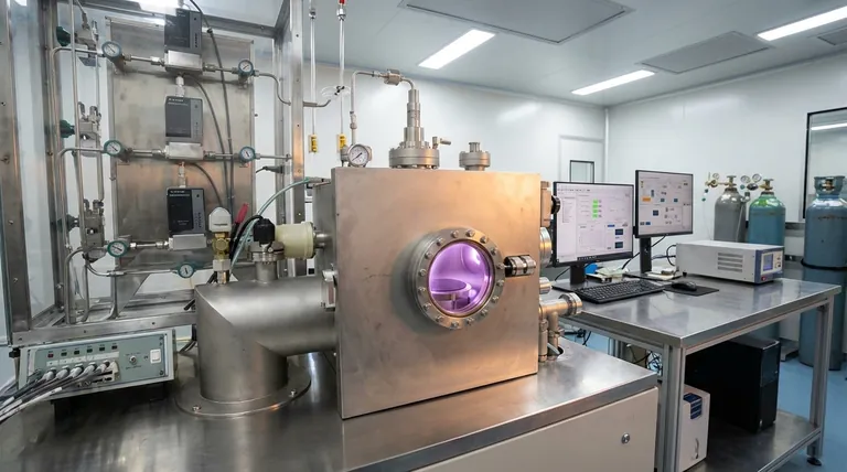
In chemistry and materials science, deposition is the process by which a material in a gaseous or plasma state transitions directly into a solid, forming a thin layer on a surface, known as a substrate. It is the fundamental process used to create thin films, which are critical components in everything from microchips to medical implants. Essentially, it is the reverse of processes like sublimation or evaporation.
Deposition is not merely a phase change; it is a highly controlled engineering technique. The core purpose is to deposit an ultra-thin film of a specific material onto a substrate to intentionally alter its surface properties, such as its conductivity, hardness, or optical behavior.
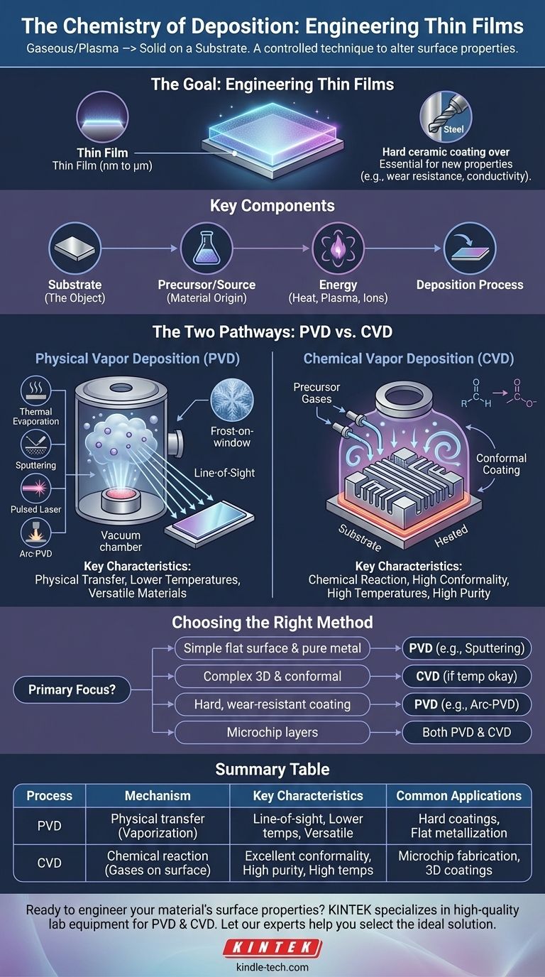
The Goal of Deposition: Engineering Thin Films
Deposition processes are designed to create thin films, which are layers of material ranging from a few atoms (nanometers) to several thousand atoms (micrometers) thick.
Why Thin Films are Essential
A thin film can grant a bulk material entirely new properties without changing its core structure. This is an incredibly efficient way to engineer a material for a specific task.
For example, a hard, wear-resistant coating can be deposited onto a standard steel drill bit, dramatically increasing its lifespan and performance. The bulk of the drill bit remains tough, inexpensive steel, while the surface gains the properties of a much harder ceramic.
The Key Components of Deposition
Every deposition process involves three core elements:
- Substrate: The object or material onto which the film is being deposited.
- Precursor/Source: The material that will form the film. This starts as a solid, liquid, or gas before being transported to the substrate.
- Energy: The energy source (e.g., heat, plasma, ions, photons) that drives the transformation and transport of the precursor material.
The Two Major Pathways: Physical vs. Chemical
All deposition techniques fall into one of two major categories. The distinction between them is crucial for understanding their capabilities and limitations.
Physical Vapor Deposition (PVD)
In PVD, the material to be deposited is physically converted into a vapor and transported to the substrate, where it condenses back into a solid. No chemical reaction occurs at the substrate surface.
Think of it like boiling water to create steam (vapor) that then condenses as frost on a cold window. The frost is chemically identical to the water you started with.
Common PVD techniques include:
- Thermal Evaporation: A source material is heated in a vacuum until it evaporates, and the vapor travels to and condenses on the cooler substrate.
- Sputtering: A target made of the source material is bombarded with high-energy ions (a plasma), which physically knock atoms off the target. These atoms then travel and deposit onto the substrate.
- Pulsed Laser Deposition: A high-power laser ablates (blasts away) material from a target, creating a plasma plume that deposits on the substrate.
- Cathodic Arc Deposition (Arc-PVD): A high-current electric arc is used to vaporize material from a cathode target, creating a highly ionized vapor that forms a dense film.
Chemical Vapor Deposition (CVD)
In CVD, one or more volatile precursor gases are introduced into a reaction chamber. These gases react or decompose on the heated substrate surface to produce the desired solid film.
Unlike PVD, a chemical reaction is the core of the process. The resulting film is a new material formed from the precursor gases. This is like mixing two gases that, upon contact with a hot surface, react to form a solid residue.
Understanding the Trade-offs
Choosing between PVD and CVD depends entirely on the desired film properties, the substrate material, and the geometry of the part being coated.
PVD: Directionality and Material Versatility
PVD processes are generally "line-of-sight," meaning the depositing material travels in a straight line from the source to the substrate.
This makes it difficult to uniformly coat complex, three-dimensional shapes. However, PVD can be performed at lower temperatures than many CVD processes and can deposit a vast range of materials, including metals, alloys, and many ceramics.
CVD: Conformality and Purity
Because the precursor is a gas that surrounds the object, CVD is excellent at producing highly conformal coatings that uniformly cover intricate and complex surfaces.
CVD can also produce films of extremely high purity and crystalline quality, which is critical for the semiconductor industry. Its main limitation is the typically high temperatures required, which can damage sensitive substrates, and the often hazardous nature of the precursor gases.
How to Apply This to Your Goal
The best method is determined by the required film characteristics and the substrate's limitations.
- If your primary focus is coating a simple, flat surface with a pure metal: PVD methods like sputtering or thermal evaporation are often the most direct and cost-effective.
- If your primary focus is creating a highly uniform, crystalline film on a complex 3D object: CVD is likely the superior choice, provided the substrate can tolerate the high process temperatures.
- If your primary focus is depositing a very hard, wear-resistant coating on tools: PVD techniques like sputtering or cathodic arc deposition are industry standards.
- If your primary focus is fabricating the foundational layers of a microchip: Both PVD and various forms of CVD are used extensively for different layers, chosen for their specific electrical properties and purity.
Ultimately, understanding the distinction between physical transfer (PVD) and chemical reaction (CVD) is the key to selecting the right tool for engineering a material's surface.
Summary Table:
| Process Type | Mechanism | Key Characteristics | Common Applications |
|---|---|---|---|
| Physical Vapor Deposition (PVD) | Physical transfer of material via vaporization. | Line-of-sight, lower temperatures, versatile materials. | Hard coatings for tools, flat surface metallization. |
| Chemical Vapor Deposition (CVD) | Chemical reaction of precursor gases on a hot surface. | Excellent conformality on complex shapes, high purity, high temperatures. | Microchip fabrication, uniform coatings on 3D objects. |
Ready to engineer your material's surface properties?
The right deposition process is critical for achieving the desired conductivity, hardness, or performance in your application. KINTEK specializes in providing high-quality lab equipment and consumables for both PVD and CVD processes, serving research and industrial laboratories.
Let our experts help you select the ideal solution for your substrate and thin-film goals. Contact our team today to discuss your project and discover how we can enhance your lab's capabilities.
Visual Guide
Related Products
- Chemical Vapor Deposition CVD Equipment System Chamber Slide PECVD Tube Furnace with Liquid Gasifier PECVD Machine
- Microwave Plasma Chemical Vapor Deposition MPCVD Machine System Reactor for Lab and Diamond Growth
- 915MHz MPCVD Diamond Machine Microwave Plasma Chemical Vapor Deposition System Reactor
- Customer Made Versatile CVD Tube Furnace Chemical Vapor Deposition Chamber System Equipment
- HFCVD Machine System Equipment for Drawing Die Nano-Diamond Coating
People Also Ask
- What is the chemical vapor deposition growth process? Build Superior Thin Films from the Atom Up
- Why is Chemical Vapor Deposition (CVD) equipment uniquely suited for constructing hierarchical superhydrophobic structures?
- What types of substrates are used in CVD to facilitate graphene films? Optimize Graphene Growth with the Right Catalyst
- How are carbon nanotubes grown? Master Scalable Production with Chemical Vapor Deposition
- What is plasma enhanced chemical vapor deposition PECVD equipment? A Guide to Low-Temperature Thin Film Deposition


