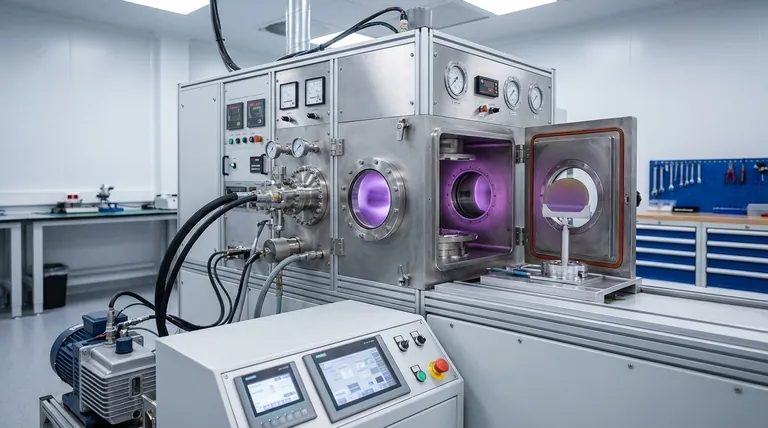
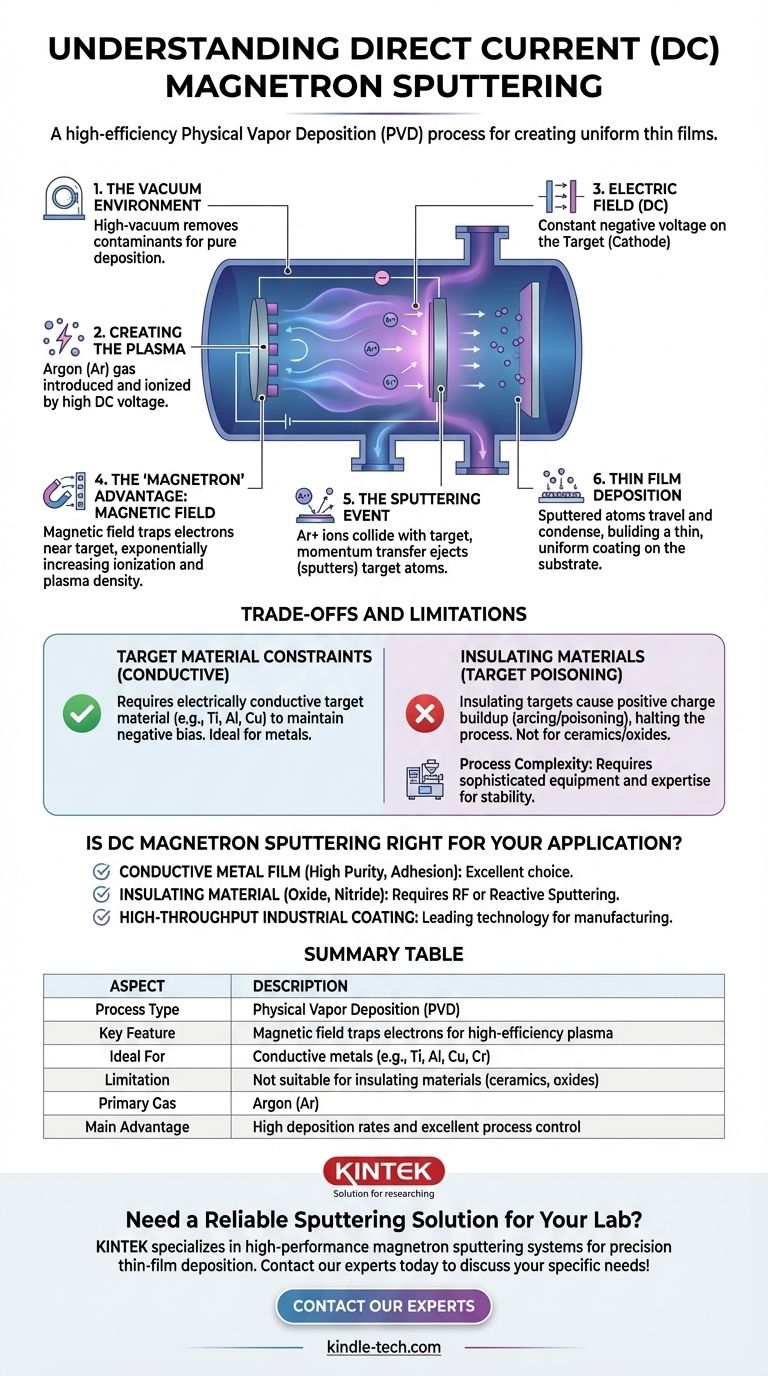
Direct current (DC) magnetron sputtering is a physical vapor deposition (PVD) process used to create high-quality, uniform thin films. It works by generating a plasma in a vacuum and using a combination of a static electric field and a magnetic field to bombard a source material (the "target") with ions. This bombardment dislodges atoms from the target, which then travel and condense onto a substrate to form the desired coating.
The defining feature of magnetron sputtering is its use of a magnetic field to trap electrons near the target material. This seemingly simple addition dramatically increases the efficiency of the plasma, leading to significantly higher deposition rates and better process control compared to basic sputtering techniques.
Deconstructing the Sputtering Process
To understand DC magnetron sputtering, it's best to break it down into its fundamental stages. Each step plays a critical role in the final quality of the thin film.
The Vacuum Environment
The entire process takes place within a sealed, high-vacuum chamber. Removing air and other gases is essential to prevent contamination of the film and to allow the sputtered atoms to travel freely from the target to the substrate.
Creating the Plasma
Once a vacuum is achieved, a small amount of an inert gas—most commonly argon (Ar)—is introduced into the chamber at low pressure. A high DC voltage is then applied between two electrodes: the cathode (which is the target) and the anode. This high voltage ionizes the argon gas, stripping electrons from the argon atoms and creating a mixture of positive argon ions (Ar+) and free electrons. This ionized gas is the plasma, often visible as a characteristic glow.
The Role of the Electric Field (DC)
The "direct current" aspect means a constant negative voltage is applied to the target material (the cathode). The positively charged argon ions in the plasma are naturally accelerated by this electric field and drawn aggressively toward the negatively charged target.
The 'Magnetron' Advantage: The Magnetic Field
This is the key innovation. A strong, permanent magnetic field is positioned behind the target. This magnetic field does not directly affect the heavy argon ions, but it has a profound effect on the light, negatively charged electrons.
The field traps these electrons in a cycloidal path close to the face of the target. By forcing them to travel a much longer path instead of escaping, the probability of them colliding with and ionizing neutral argon atoms increases exponentially. This creates a much denser, more intense plasma precisely where it is needed—right in front of the target.
The Sputtering Event
The dense cloud of positive argon ions, accelerated by the electric field, collides with the target surface with significant energy. Each collision acts like a microscopic billiard ball break, transferring momentum and ejecting, or "sputtering," atoms from the target material.
Thin Film Deposition
These newly freed, neutral atoms from the target material travel in a straight line through the low-pressure environment. When they encounter the substrate (the object being coated), they condense on its surface, gradually building up a thin, uniform film.
Understanding the Trade-offs and Limitations
While powerful, DC magnetron sputtering is not a universal solution. Its core mechanism imposes specific constraints that are critical to understand.
Target Material Constraints
The primary limitation of the DC method is that the target material must be electrically conductive. A constant negative charge must be maintained on the target to attract the positive ions.
If you attempt to sputter an insulating or dielectric material (like a ceramic or an oxide), positive charge from the arriving ions quickly builds up on the target's surface. This effect, known as target poisoning or arcing, neutralizes the negative bias and effectively shuts down the sputtering process.
Process Complexity
Magnetron sputtering systems are sophisticated pieces of equipment. They require high-vacuum pumps, precise gas flow controllers, high-voltage DC power supplies, and carefully engineered magnetic arrays. Achieving a stable and repeatable process requires significant expertise and control.
Is DC Magnetron Sputtering Right for Your Application?
The decision to use this technique hinges entirely on your material requirements and production goals.
- If your primary focus is depositing a conductive metal film with high purity and good adhesion: DC magnetron sputtering is an industry-standard, efficient, and highly reliable choice for materials like titanium, aluminum, copper, or chromium.
- If your primary focus is depositing an insulating material like an oxide or nitride: You will need to look beyond DC sputtering to techniques like RF (Radio Frequency) sputtering or reactive sputtering, which are designed to overcome the issue of charge buildup.
- If your primary focus is high-throughput industrial coating: The high deposition rates and scalability of magnetron sputtering make it a leading technology for manufacturing applications, such as coating architectural glass or producing microelectronics.
Understanding the principles of how the magnetic field enhances the plasma is the key to effectively leveraging this powerful thin-film deposition technology.
Summary Table:
| Aspect | Description |
|---|---|
| Process Type | Physical Vapor Deposition (PVD) |
| Key Feature | Magnetic field traps electrons for high-efficiency plasma |
| Ideal For | Conductive metals (e.g., Ti, Al, Cu, Cr) |
| Limitation | Not suitable for insulating materials (ceramics, oxides) |
| Primary Gas Used | Argon (Ar) |
| Main Advantage | High deposition rates and excellent process control |
Need a reliable sputtering solution for your lab? KINTEK specializes in high-performance lab equipment, including magnetron sputtering systems designed for precision thin-film deposition. Whether you're working with conductive metals or exploring advanced materials, our expertise ensures you get the right equipment for superior results. Contact our experts today to discuss your specific laboratory needs and discover how KINTEK can enhance your research and production capabilities!
Visual Guide
Related Products
- Chemical Vapor Deposition CVD Equipment System Chamber Slide PECVD Tube Furnace with Liquid Gasifier PECVD Machine
- Microwave Plasma Chemical Vapor Deposition MPCVD Machine System Reactor for Lab and Diamond Growth
- HFCVD Machine System Equipment for Drawing Die Nano-Diamond Coating
- Customer Made Versatile CVD Tube Furnace Chemical Vapor Deposition Chamber System Equipment
- 915MHz MPCVD Diamond Machine Microwave Plasma Chemical Vapor Deposition System Reactor
People Also Ask
- Why is Chemical Vapor Deposition (CVD) equipment uniquely suited for constructing hierarchical superhydrophobic structures?
- What are the advantages of chemical vapor deposition? Achieve Superior Thin Films for Your Lab
- What are the processes of vapor phase deposition? Understand CVD vs. PVD for Superior Thin Films
- What types of substrates are used in CVD to facilitate graphene films? Optimize Graphene Growth with the Right Catalyst
- What is plasma enhanced chemical vapor deposition PECVD equipment? A Guide to Low-Temperature Thin Film Deposition


