Epitaxial growth of graphene is a process where a single, highly-ordered layer of graphene is grown on the surface of a crystalline substrate, which acts as a template for the atoms. This method forces the carbon atoms to arrange themselves into graphene's characteristic honeycomb lattice, resulting in a large, high-quality sheet with minimal defects.
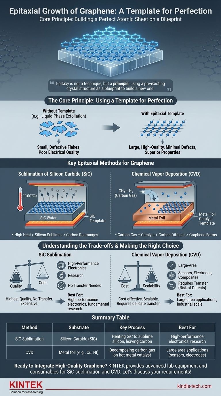
The core concept to understand is that epitaxy is not one specific technique, but a principle of using a pre-existing crystal structure as a blueprint to build a new one. For graphene, this is primarily achieved through either the sublimation of Silicon Carbide (SiC) or Chemical Vapor Deposition (CVD) on a metal catalyst.
The Core Principle: Using a Template for Perfection
To harness graphene's extraordinary electronic and mechanical properties, its atomic structure must be as close to perfect as possible. Epitaxial growth is the leading strategy to achieve this level of control over large areas.
What is Epitaxy?
Epitaxy is the process of depositing or growing a crystalline film on top of a crystalline substrate. The substrate's own atomic lattice acts as a template, guiding the atoms of the new layer to align in a specific, ordered orientation.
Think of it like laying perfectly aligned tiles on a floor that already has a grid pattern. The grid ensures every new tile is placed correctly, creating a flawless, large-scale pattern.
Why This is Critical for Graphene
Graphene's value comes from its defect-free honeycomb structure. Methods like liquid-phase exfoliation can produce large quantities of graphene flakes, but they are often small and contain many defects, which degrades their electrical quality.
Epitaxy solves this by building the graphene sheet atom-by-atom in a controlled environment, drastically reducing structural flaws.
Key Epitaxial Methods for Graphene
While the principle is the same, two dominant methods are used to apply it for graphene production.
Sublimation of Silicon Carbide (SiC)
In this method, a wafer of Silicon Carbide (SiC) is heated to very high temperatures (over 1100°C) in a vacuum.
The intense heat causes the silicon atoms to sublimate (turn directly from a solid into a gas), leaving the surface.
The carbon atoms left behind then restructure themselves on the SiC crystal template, forming a high-quality layer of epitaxial graphene directly on the wafer.
Chemical Vapor Deposition (CVD)
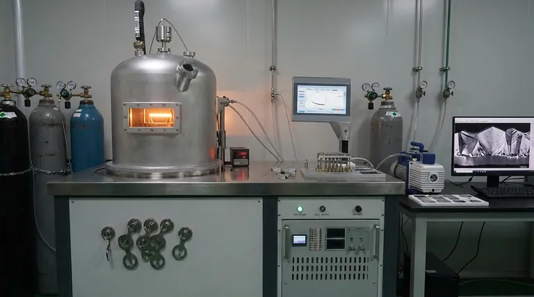
CVD is the most common method for large-scale production. It involves placing a substrate, typically a transition metal foil like copper or nickel, in a furnace.
A carbon-containing gas, such as methane (CH₄), is then introduced. The hot metal surface acts as a catalyst, breaking down the methane molecules.
The released carbon atoms then diffuse and assemble on the metal's surface, using the metal's crystal lattice as a guide to form a continuous sheet of graphene.
Understanding the Trade-offs
Choosing a growth method involves balancing quality, cost, and usability. There is no single "best" method; the choice depends entirely on the final application.
Quality vs. Cost
Graphene grown on SiC is exceptionally high-quality and is already on a semiconducting substrate, making it ideal for high-performance electronics. However, SiC wafers are extremely expensive, limiting this method to research and specialized applications.
CVD is far more cost-effective and can produce graphene sheets measured in square meters. This makes it the leading candidate for industrial-scale applications.
Scalability vs. The Transfer Problem
The primary advantage of CVD is its scalability. However, its greatest challenge is that the graphene is grown on a metal foil.
For most electronic applications, the graphene must be delicately transferred from the metal catalyst onto a different substrate, like silicon. This transfer process is notorious for introducing wrinkles, tears, and contaminants that can compromise the graphene's quality.
Making the Right Choice for Your Goal
The optimal growth strategy is defined by the needs of your project.
- If your primary focus is fundamental research or high-performance electronics: Epitaxial growth on SiC is often the superior choice because it provides the highest quality graphene on a non-conductive substrate, with no transfer required.
- If your primary focus is large-area applications like transparent electrodes, sensors, or composites: CVD is the only practical method due to its scalability and significantly lower cost, even when accounting for the challenges of the transfer process.
Ultimately, mastering epitaxial growth is key to moving graphene from a laboratory marvel to a transformative industrial material.
Summary Table:
| Method | Substrate | Key Process | Best For |
|---|---|---|---|
| SiC Sublimation | Silicon Carbide (SiC) | Heating SiC to sublime silicon, leaving carbon to form graphene | High-performance electronics, research |
| Chemical Vapor Deposition (CVD) | Metal foil (e.g., Copper, Nickel) | Decomposing carbon gas on a hot metal catalyst | Large-area applications (sensors, electrodes, composites) |
Ready to Integrate High-Quality Graphene into Your Research or Product Development?
Choosing the right epitaxial growth method is critical for achieving the material properties your project demands. KINTEK specializes in providing the advanced lab equipment and consumables necessary for both SiC sublimation and CVD processes. Our expertise ensures you have the reliable tools needed to produce high-quality, large-area graphene for applications in electronics, sensing, and composites.
Let's discuss your specific requirements. Contact our experts today to find the perfect solution for your laboratory's needs.
Visual Guide
Related Products
- Microwave Plasma Chemical Vapor Deposition MPCVD Machine System Reactor for Lab and Diamond Growth
- 915MHz MPCVD Diamond Machine Microwave Plasma Chemical Vapor Deposition System Reactor
People Also Ask
- How do vacuum pumps and valves collaborate in MPCVD? Achieve Precise Pressure Control for Superior CNT Synthesis
- Why is argon-rich gas phase chemistry used for UNCD growth? Unlock Precision Nano-Diamond Synthesis
- How does a microwave plasma reactor facilitate the synthesis of diamond? Master MPCVD with Precision Technology
- What is microwave plasma chemical vapor deposition? A Guide to High-Purity Diamond Film Growth
- What are the primary advantages of the CVD method for growing diamonds? Engineering High-Purity Gems and Components

