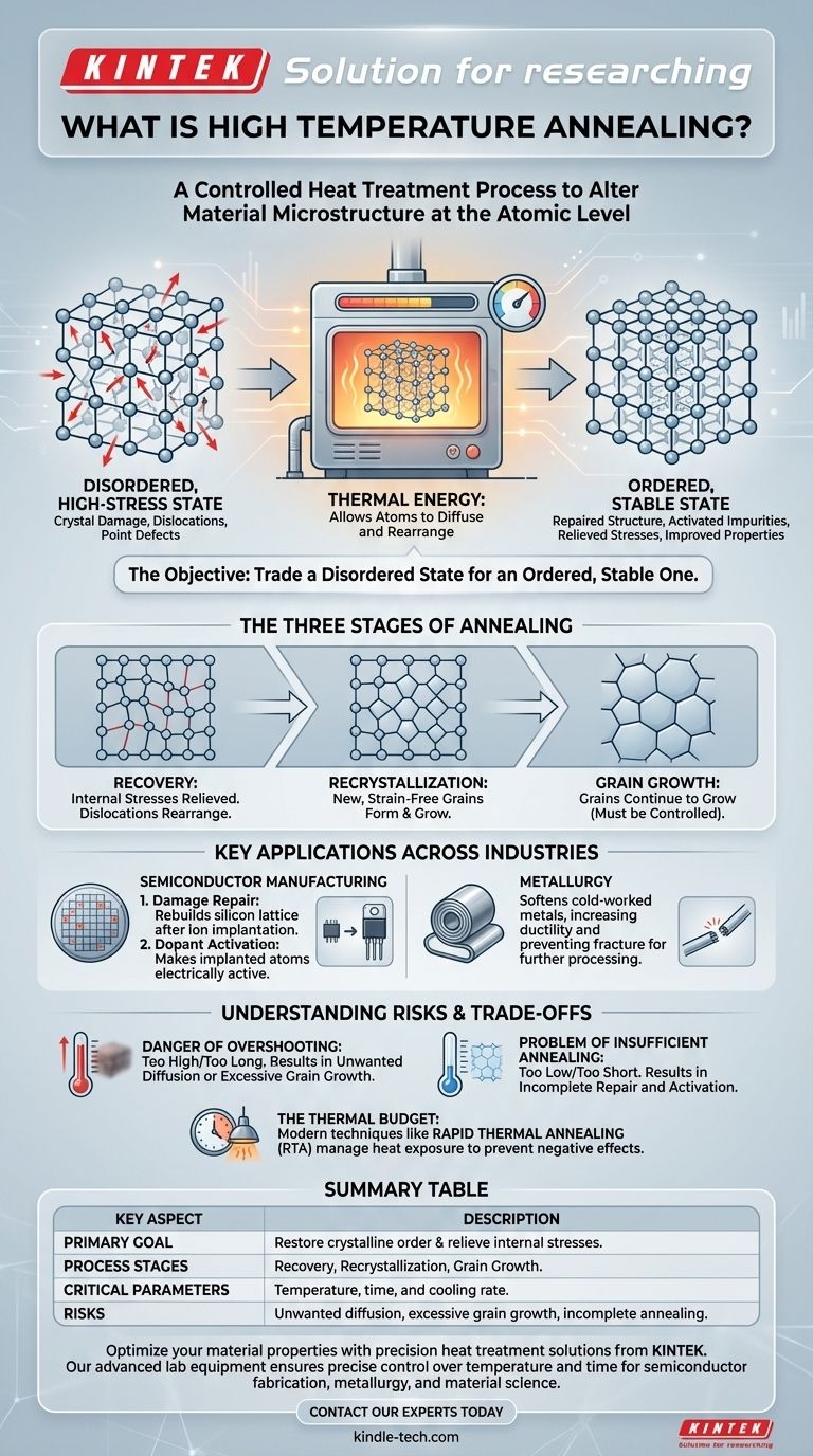
At its core, high temperature annealing is a controlled heat treatment process used to fundamentally alter a material's internal microstructure. This carefully managed thermal cycle—heating to a specific high temperature, holding it there, and then cooling it—is not about melting the material, but about giving its atoms enough energy to move and rearrange themselves. The primary goals are to repair crystal damage, activate impurities, and relieve internal stresses, thereby improving critical properties like ductility and electrical conductivity.
High temperature annealing is a precision engineering tool used to repair a material's internal crystal structure. The objective is to trade a disordered, high-stress state for an ordered, stable one, thereby unlocking the material's desired physical and electrical properties.
The Fundamental Goal: Restoring Crystalline Order
High temperature annealing is fundamentally a process of thermodynamic optimization. It allows a material to move from a high-energy, disordered state to a more stable, lower-energy, and more useful state.
What "Damage" Are We Fixing?
Materials are rarely perfect. Processes like cold working in metals or ion implantation in semiconductors introduce significant disorder into the crystal lattice.
This damage manifests as dislocations, which are misalignments in the crystal structure, or point defects, where atoms are missing or in the wrong place. These defects act as roadblocks, impeding electron flow or making a material brittle.
The Role of Thermal Energy
Heat provides the kinetic energy necessary for atoms to overcome their local energy barriers.
By raising the temperature, we allow atoms to vibrate more intensely and diffuse, or move, through the lattice. This mobility enables them to settle back into their proper, low-energy positions, effectively "healing" the defects.
The Three Stages of Annealing
The process can be broadly understood in three phases:
- Recovery: Internal stresses are relieved as dislocations within the crystal rearrange themselves into lower-energy configurations.
- Recrystallization: New, strain-free grains begin to form and grow, replacing the deformed, high-defect grains.
- Grain Growth: After recrystallization is complete, the new grains may continue to grow larger. This must be carefully controlled, as excessively large grains can sometimes be detrimental.
Key Applications Across Industries
While the principles are universal, the specific application of high temperature annealing is tailored to the industry and the material.
In Semiconductor Manufacturing
This is one of the most critical applications. After ions (dopants like boron or phosphorus) are shot into a silicon wafer during ion implantation, the crystal lattice is severely damaged.
High temperature annealing achieves two essential goals here:
- Damage Repair: It provides the energy to rebuild the silicon crystal lattice.
- Dopant Activation: It allows the implanted dopant atoms to move into substitutional sites within the lattice, where they can donate or accept electrons and become electrically active. Without this step, the dopants would be useless.
In Metallurgy
After a metal is mechanically deformed (a process known as cold working), it becomes harder but also more brittle due to an increase in dislocations.
Annealing is used to reverse this effect, making the metal softer and more ductile (able to be drawn into a wire or shaped). This allows for further processing without the risk of fracture.
Understanding the Trade-offs and Risks
High temperature annealing is a process of precision. Deviating from the optimal parameters can create new problems instead of solving existing ones.
The Danger of Overshooting
Using a temperature that is too high or holding it for too long can be highly detrimental.
In semiconductors, this leads to unwanted dopant diffusion, blurring the sharp boundaries of the microscopic transistors you are trying to create. In metals, it can cause excessive grain growth, which can reduce the material's strength.
The Problem of Insufficient Annealing
Conversely, if the temperature is too low or the time is too short, the process will be incomplete.
Crystal damage will remain, and dopants in a semiconductor will not be fully activated. This results in devices and materials that fail to meet their performance specifications.
The Concept of a Thermal Budget
In semiconductor fabrication, every high-temperature step consumes a portion of the "thermal budget." This is the total amount of heat a device can be exposed to before negative effects, like diffusion, begin to compromise its structure.
Modern techniques like Rapid Thermal Annealing (RTA) were developed specifically to manage this. RTA uses high-intensity lamps to heat a wafer to very high temperatures in seconds, accomplishing the anneal before significant diffusion can occur.
Making the Right Choice for Your Process
The ideal annealing strategy is dictated entirely by your material and your final goal.
- If your primary focus is activating dopants in modern semiconductors: You need a short-duration process like Rapid Thermal Annealing (RTA) to maximize activation while minimizing dopant diffusion.
- If your primary focus is softening a large metal part for formability: A slower, more traditional furnace anneal is the correct approach to ensure uniform heating and stress relief throughout the bulk material.
- If your primary focus is repairing widespread crystal damage after ion implantation: The temperature and duration must be carefully optimized to allow lattice repair without causing unwanted side effects like dopant clustering.
Ultimately, mastering high temperature annealing means treating it not as simple heating, but as a precision tool for engineering materials at the atomic level.
Summary Table:
| Key Aspect | Description |
|---|---|
| Primary Goal | Restore crystalline order and relieve internal stresses. |
| Process Stages | Recovery, Recrystallization, Grain Growth. |
| Common Applications | Semiconductor dopant activation, metal softening, crystal damage repair. |
| Critical Parameters | Temperature, time, and cooling rate. |
| Risks | Unwanted dopant diffusion, excessive grain growth, incomplete annealing. |
Optimize your material properties with precision heat treatment solutions from KINTEK.
High temperature annealing is a critical step for achieving the desired electrical and mechanical performance in semiconductors and metals. Whether you need to activate dopants with Rapid Thermal Annealing (RTA) or soften metal parts for formability, KINTEK's advanced lab equipment ensures precise control over temperature and time.
Our expertise in lab equipment and consumables supports researchers and manufacturers in:
- Semiconductor Fabrication: Achieve high dopant activation with minimal diffusion.
- Metallurgy: Enhance ductility and relieve stresses in cold-worked metals.
- Material Science: Repair crystal damage and optimize grain structure.
Let KINTEK help you master this atomic-level engineering process. Contact our experts today to discuss your specific annealing requirements and discover the right equipment for your laboratory.
Visual Guide
Related Products
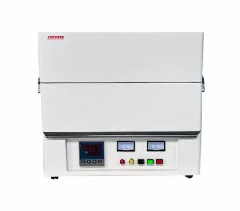
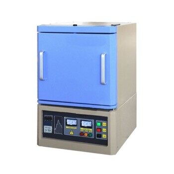
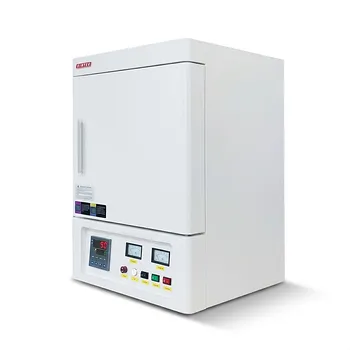
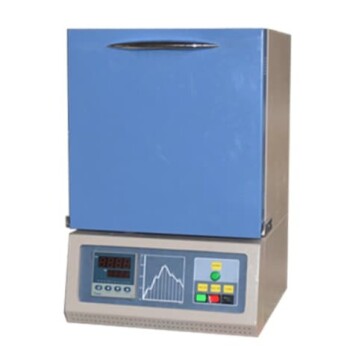
- High Temperature Muffle Oven Furnace for Laboratory Debinding and Pre Sintering
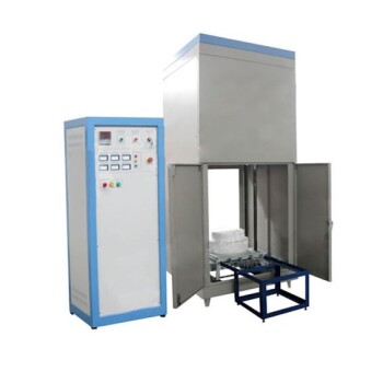
- 1700℃ Laboratory High Temperature Tube Furnace with Alumina Tube
- 1400℃ Laboratory High Temperature Tube Furnace with Alumina Tube
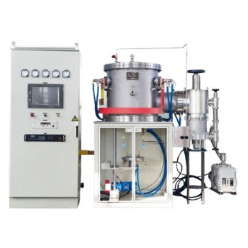
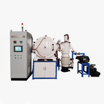
- Vacuum Heat Treat and Pressure Sintering Furnace for High Temperature Applications
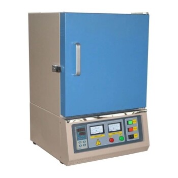
- 1400℃ Controlled Atmosphere Furnace with Nitrogen and Inert Atmosphere
People Also Ask
- What role does a high-temperature muffle furnace play in the synthesis of manganese/cobalt-modified ceramic catalysts?
- What are the main components of a high-temperature muffle furnace? A Guide to the Core Systems
- What is the significance of integrating a high-temperature muffle furnace into an impact wear testing system?
- What is the primary function of high-temperature muffle or tube furnaces for ceramic coatings? Ensure Peak Durability
- What function does a high-temperature muffle furnace serve in Ti3AlC2 MAX phase synthesis? Master Molten Salt Diffusion