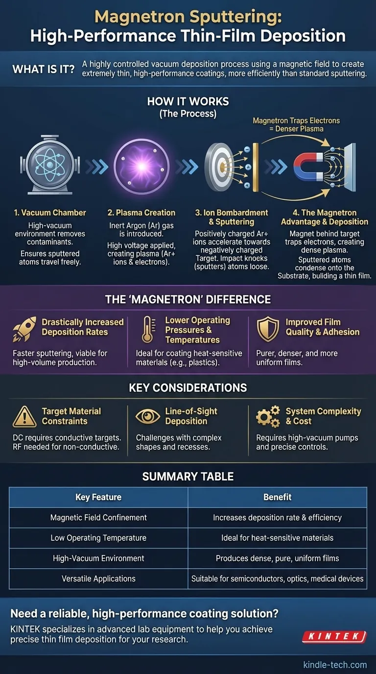
In essence, magnetron sputtering is a highly controlled vacuum deposition process used to create extremely thin, high-performance coatings. It works by bombarding a source material (the "target") with energized gas ions inside a vacuum chamber. What makes this method unique is the strategic use of a magnetic field to intensify the process, resulting in faster and more efficient deposition than standard sputtering.
The core problem with basic sputtering is its low efficiency. Magnetron sputtering solves this by using a magnetic field to trap electrons near the source material, which dramatically increases the density of the ion plasma and, consequently, the speed and quality of the coating process.
Deconstructing the Magnetron Sputtering Process
To truly understand magnetron sputtering, it's best to break it down into its fundamental stages. Each step builds upon the last to create a highly refined and powerful coating environment.
The Foundation: The Vacuum Chamber
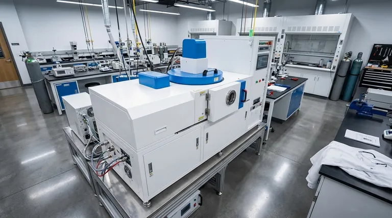
All sputtering occurs within a high-vacuum chamber. This environment is critical because it removes air and other contaminants that could interfere with the coating process or become embedded in the film, compromising its purity.
The vacuum also ensures the sputtered atoms can travel from the source to the part being coated with minimal collisions, a concept known as a long "mean free path."
Creating the Plasma: Gas and Voltage
Once a vacuum is established, a small, precisely controlled amount of an inert gas—typically Argon—is introduced into the chamber.
A high voltage is then applied, creating a powerful electric field. This field energizes the chamber, stripping electrons from the Argon atoms and creating a state of matter called plasma: a glowing, ionized gas consisting of positive Argon ions and free electrons.
The Core Mechanism: Ion Bombardment
The source material, known as the target, is given a strong negative charge. The positively charged Argon ions in the plasma are naturally accelerated by the electric field and violently collide with this negatively charged target.
Each impact has enough energy to knock atoms loose from the target's surface. This ejection of atoms is the "sputtering" effect. These neutral, sputtered atoms then travel through the vacuum and condense onto the substrate (the part being coated), gradually building up a thin film.
The 'Magnetron' Advantage: Confining the Plasma
This is the key innovation. A powerful magnet (the "magnetron") is placed behind the target. This magnetic field does not affect the neutral Argon atoms or the heavy Argon ions significantly. However, it has a profound effect on the light, negatively charged electrons.
The magnetic field traps the electrons, forcing them into a spiral path directly in front of the target surface. Instead of escaping into the chamber, these trapped electrons collide with many more neutral Argon atoms, creating a far denser and more intense plasma right where it is needed most.
Why the Magnetic Field Is a Game-Changer
The addition of the magnetic field isn't a minor tweak; it fundamentally transforms the sputtering process, delivering several critical advantages over simpler methods.
Drastically Increased Deposition Rates
By creating a much denser plasma, the number of ions bombarding the target per second increases exponentially. This directly translates to a much faster rate of sputtering and, therefore, a significantly faster coating process, making it viable for high-volume industrial production.
Lower Operating Pressures and Temperatures
Because the magnetic field makes the ionization process so efficient, magnetron sputtering can operate at much lower gas pressures. Furthermore, by trapping electrons at the target, it prevents them from bombarding the substrate. This keeps the substrate much cooler, making the process ideal for coating heat-sensitive materials like plastics, polymers, and delicate electronics.
Improved Film Quality and Adhesion
The high-density plasma and high-vacuum environment result in a deposited film that is purer, denser, and more uniform. The energetic arrival of sputtered atoms can also improve the film's adhesion to the substrate surface, leading to more durable and reliable coatings.
Understanding the Trade-offs
While powerful, magnetron sputtering is not a universal solution. Understanding its limitations is key to using it effectively.
Target Material Constraints
The most common form, DC magnetron sputtering, requires the target material to be electrically conductive. Coating non-conductive materials like ceramics requires a more complex and often slower setup known as RF (Radio Frequency) sputtering.
Line-of-Sight Deposition
The sputtered atoms travel in a relatively straight line from the target to the substrate. This makes it challenging to uniformly coat complex, three-dimensional shapes with deep recesses or undercuts without sophisticated part-rotation systems.
System Complexity and Cost
Magnetron sputtering systems are complex machines requiring high-vacuum pumps, precise gas handling, high-voltage power supplies, and the magnetron cathodes themselves. This represents a higher initial investment compared to simpler deposition techniques like electroplating.
Making the Right Choice for Your Goal
Selecting a coating process depends entirely on your end goal. Magnetron sputtering excels in specific scenarios.
- If your primary focus is high-throughput production: The high deposition rates of magnetron sputtering make it ideal for industrial-scale coating of items like architectural glass, hard drives, and solar panels.
- If your primary focus is coating delicate substrates: The process's low operating temperature protects heat-sensitive materials like polymers, optics, or fully assembled electronic components.
- If your primary focus is creating dense, high-purity films: The controlled, high-vacuum environment results in superior film quality for demanding applications in semiconductors, medical devices, and wear-resistant tools.
By understanding the fundamental role of the magnetic field, you can effectively leverage magnetron sputtering to achieve precise, high-performance coatings for your specific application.
Summary Table:
| Key Feature | Benefit |
|---|---|
| Magnetic Field Confinement | Dramatically increases deposition rate and process efficiency |
| Low Operating Temperature | Ideal for coating heat-sensitive materials (plastics, electronics) |
| High-Vacuum Environment | Produces dense, pure, and uniform films with excellent adhesion |
| Versatile Applications | Suitable for semiconductors, medical devices, optics, and wear-resistant coatings |
Need a reliable, high-performance coating solution for your laboratory?
KINTEK specializes in advanced lab equipment, including sputtering systems, to help you achieve precise and efficient thin film deposition. Whether you are working with delicate electronics, developing new semiconductor materials, or require durable coatings for research, our expertise ensures you get the right setup for your specific application.
Contact our experts today via our form to discuss how our solutions can enhance your research and development process.
Visual Guide
Related Products
- Spark Plasma Sintering Furnace SPS Furnace
- RF PECVD System Radio Frequency Plasma-Enhanced Chemical Vapor Deposition RF PECVD
People Also Ask
- What is the difference between spark plasma sintering and flash sintering? A Guide to Advanced Sintering Methods
- What is SPS sintering method? A Guide to High-Speed, High-Performance Material Fabrication
- Why are Spark Plasma Sintering (SPS) furnaces or hot presses utilized in the preparation of Li3PS4 solid electrolytes?
- What are the advantages of CAMI/SPS for W-Cu composite preparation? Reduce cycles from hours to seconds.
- What technical advantages does a Spark Plasma Sintering (SPS) furnace offer for LZP ceramics? Enhance Ionic Conductivity

