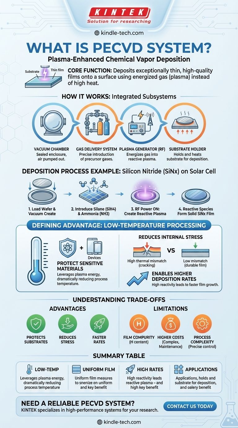
At its core, a PECVD system is a machine that deposits exceptionally thin layers of material onto a surface. It stands for Plasma-Enhanced Chemical Vapor Deposition. Unlike traditional methods that rely on high heat, PECVD uses an energized gas, or plasma, to drive the chemical reactions needed to create the film, allowing the entire process to occur at much lower temperatures.
PECVD leverages plasma to bypass the high-temperature requirements of conventional deposition. This fundamental advantage enables the creation of high-quality, uniform thin films on substrates that would otherwise be damaged by heat, broadening the scope of advanced materials engineering.
How a PECVD System Works
A PECVD system is a sophisticated assembly of integrated subsystems, each performing a critical function to achieve a controlled and precise film deposition. The process is a carefully orchestrated sequence within a highly controlled environment.
The Core Components
Every PECVD system is built around four primary components.
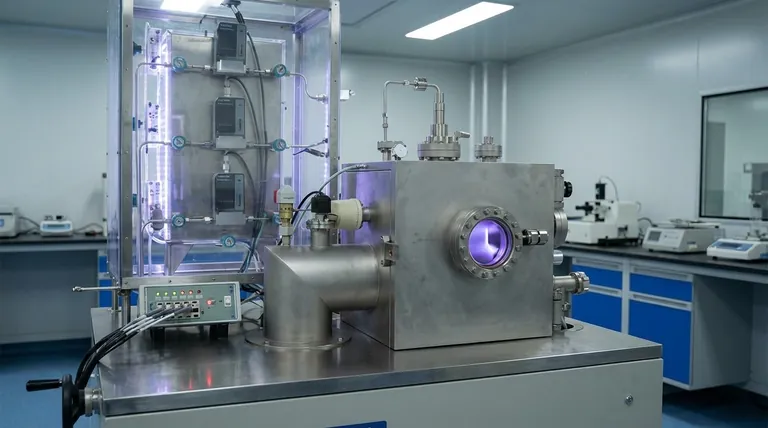
- Vacuum Chamber: This is the sealed enclosure where the deposition takes place. All air is pumped out to create a vacuum, ensuring no unwanted particles or gases contaminate the film.
- Gas Delivery System: This network of pipes and valves precisely introduces specific precursor gases (the raw ingredients for the film) into the vacuum chamber at controlled flow rates.
- Plasma Generator: Typically an RF (Radio Frequency) power supply, this component energizes the precursor gases inside the chamber, stripping electrons from the atoms and creating a glowing, reactive plasma.
- Substrate Holder: This stage holds the material to be coated, known as the substrate (e.g., a silicon wafer). It is often heated to a moderate temperature to improve film quality and adhesion.
The Deposition Process in Action
The process follows a clear sequence. For example, to create a silicon nitride (SiNx) anti-reflection layer on a solar cell:
- A silicon wafer (the substrate) is placed in the chamber, and a vacuum is created.
- Precursor gases, such as silane (SiH4) and ammonia (NH3), are introduced.
- The RF power supply is turned on, creating a glow discharge plasma that decomposes the gas molecules into highly reactive species.
- These reactive species then combine on the surface of the wafer, forming a solid, thin film of silicon nitride.
The Defining Advantage: Low-Temperature Processing
The use of plasma is not just a technical detail; it is the central benefit that defines PECVD and its applications. By using plasma energy instead of thermal energy, the process temperature can be dramatically reduced.
Protecting the Substrate
Many advanced materials, including certain polymers or devices with pre-existing metallic layers, cannot withstand the high temperatures of traditional deposition methods. PECVD's low-temperature nature prevents thermal damage, making it an essential tool for complex device fabrication.
Reducing Internal Stress
When a film and a substrate are heated and cooled at different rates, it creates stress that can cause the film to crack or peel. By minimizing the overall process temperature, PECVD significantly reduces this thermal mismatch, leading to more durable and reliable films.
Enabling Higher Deposition Rates
The high reactivity of the species within the plasma can lead to significantly faster film growth compared to many low-temperature alternatives. This is especially beneficial for creating thicker amorphous or microcrystalline films where throughput is a key concern.
Understanding the Trade-offs
While powerful, PECVD is not a universal solution. Understanding its limitations is critical for making an informed decision.
Film Composition and Purity
Because the precursor gases (like silane) are often hydrogen-based, a common issue with PECVD is the incorporation of hydrogen into the final film. This can affect the material's electrical and optical properties and may require subsequent annealing steps to remove.
Equipment and Maintenance Costs
PECVD systems are complex machines. The vacuum pumps, RF generators, and control systems require significant capital investment and regular, specialized maintenance, leading to higher operational costs compared to simpler methods.
Process Complexity
Achieving a perfectly uniform film across a large substrate requires precise control over gas flow, pressure, plasma power, and temperature. Optimizing this multi-variable process can be complex and time-consuming.
Making the Right Choice for Your Application
Selecting the appropriate deposition technology depends entirely on the specific requirements of your material, device, and production goals.
- If your primary focus is processing temperature-sensitive materials: PECVD is the default choice, as its low-temperature nature prevents substrate damage.
- If your primary focus is maximum throughput: Certain PECVD variants, like Microwave or VHF-PECVD, are specifically designed for high deposition rates.
- If your primary focus is ultimate film purity and density: You may need to consider higher-temperature methods or specific PECVD types (like MWECR-PECVD) that produce higher-quality films, and weigh that against thermal budget constraints.
Ultimately, PECVD provides a versatile and powerful toolset for depositing critical thin films that are foundational to modern electronics, optics, and energy technologies.
Summary Table:
| Feature | Description | Key Benefit |
|---|---|---|
| Low-Temperature Processing | Uses plasma instead of high heat for deposition. | Protects heat-sensitive substrates (e.g., polymers, pre-fabricated devices). |
| Uniform Film Deposition | Precise control over gas flow, pressure, and plasma power. | Ensures consistent film quality across large surfaces. |
| High Deposition Rates | Reactive plasma species accelerate film growth. | Improves throughput for thicker amorphous or microcrystalline films. |
| Common Applications | Silicon nitride anti-reflection coatings, MEMS, semiconductors. | Enables advanced materials engineering in electronics and optics. |
Need a reliable PECVD system for your lab? KINTEK specializes in lab equipment and consumables, providing high-performance PECVD systems tailored to your research or production needs. Whether you're working with temperature-sensitive substrates or require high deposition rates, our expertise ensures you get the right solution for precise thin film deposition. Contact us today to discuss how we can support your laboratory goals!
Visual Guide
Related Products
- RF PECVD System Radio Frequency Plasma-Enhanced Chemical Vapor Deposition RF PECVD
- Chemical Vapor Deposition CVD Equipment System Chamber Slide PECVD Tube Furnace with Liquid Gasifier PECVD Machine
- Inclined Rotary Plasma Enhanced Chemical Vapor Deposition PECVD Equipment Tube Furnace Machine
- Inclined Rotary Plasma Enhanced Chemical Vapor Deposition PECVD Equipment Tube Furnace Machine
- 915MHz MPCVD Diamond Machine Microwave Plasma Chemical Vapor Deposition System Reactor
People Also Ask
- What is the role of RF-PECVD in VFG preparation? Mastering Vertical Growth and Surface Functionality
- What is plasma chemical vapor deposition? A Low-Temperature Thin Film Coating Solution
- What is an example of PECVD? RF-PECVD for High-Quality Thin Film Deposition
- How does Radio Frequency Enhanced Plasma Chemical Vapour Deposition (RF-PECVD) work? Learn the Core Principles
- What is plasma enhanced chemical vapour deposition process? Unlock Low-Temperature, High-Quality Thin Films


