In manufacturing, PVD stands for Physical Vapor Deposition. It is not a single process but a family of vacuum-based techniques used to apply exceptionally thin, high-performance films onto a surface. The fundamental principle involves transforming a solid source material into a vapor, which then travels through a vacuum chamber and condenses onto the target object, known as the substrate, to form a solid, durable coating.
Physical Vapor Deposition is a sophisticated surface engineering tool. Its primary purpose is to enhance an object's properties—such as hardness, wear resistance, or conductivity—by depositing a microscopic layer of a specific material without altering the object's core structure.

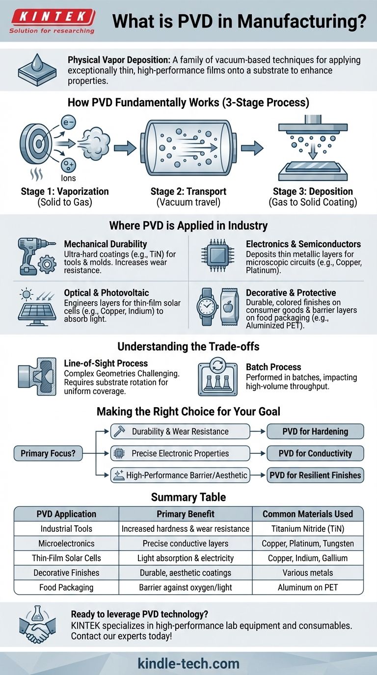
How PVD Fundamentally Works
The PVD process, while varied in its specific techniques like sputtering or evaporation, follows a consistent three-stage sequence within a controlled vacuum chamber.
Stage 1: Vaporization
The process begins by converting a solid source material, often called a "target," into a gaseous vapor. This is achieved using high-energy methods, such as bombarding the target with ions (sputtering) or heating it until it evaporates.
Stage 2: Transport
Once vaporized, the atoms or molecules of the coating material travel through the vacuum chamber. The vacuum is critical because it removes other atmospheric particles that could contaminate the coating or impede the vapor's path to the substrate.
Stage 3: Deposition
When the vapor cloud reaches the cooler surface of the substrate (the part being coated), it condenses back into a solid state. This forms a thin, highly-adherent, and uniform film across the surface of the object.
Where PVD is Applied in Industry
PVD's versatility allows it to be used across numerous high-tech industries for a wide range of functions, from mechanical to electronic.
For Mechanical Durability
The most well-known application is creating ultra-hard coatings for industrial tools. A thin layer of a material like Titanium Nitride (TiN) dramatically increases the wear resistance and lifespan of cutting tools, drills, and molds.
For Electronics and Semiconductors
PVD is essential in microfabrication. It is used to deposit the thin metallic layers (like copper, platinum, or tungsten) that form the microscopic circuits on silicon wafers for microchips and other semiconductor devices.
For Optical and Photovoltaic Functions
In the production of thin-film solar cells, PVD is used to deposit layers of materials like copper, indium, or gallium. These layers are engineered to have specific properties for absorbing light and generating electricity.
For Decorative and Protective Finishes
PVD is also used for consumer products. The thin, metallic layer on food packaging like potato chip bags (aluminized PET film) is often applied via PVD, providing a barrier to oxygen and light. It is also used to create durable, colored finishes on watches, faucets, and other hardware.
Understanding the Trade-offs
While powerful, PVD is a line-of-sight process. This means the coating material travels in a straight line from the source to the substrate.
Complex Geometries Can Be a Challenge
Coating the inside of deep holes or complex, shadowed internal features can be difficult. The substrate often needs to be rotated and repositioned during the process to ensure complete and uniform coverage.
It Is a Batch Process
Unlike a continuous production line, PVD is typically performed in batches. Parts must be loaded into the vacuum chamber, the process run, and the chamber then vented to retrieve the finished parts. This can impact throughput for very high-volume manufacturing.
Making the Right Choice for Your Goal
When deciding if PVD is the correct approach, consider the primary property you need to engineer on your part's surface.
- If your primary focus is durability and wear resistance: PVD is an industry-standard solution for hardening the surfaces of tools and high-wear mechanical components.
- If your primary focus is creating precise electronic properties: PVD offers the high level of purity and control needed to deposit conductive or semiconductive films for microelectronics.
- If your primary focus is a high-performance barrier or aesthetic finish: PVD provides a uniform and resilient coating for applications ranging from protective food packaging to durable luxury finishes.
Ultimately, PVD empowers engineers to give a material surface properties that its bulk form does not possess.
Summary Table:
| PVD Application | Primary Benefit | Common Materials Used |
|---|---|---|
| Industrial Tools | Increased hardness & wear resistance | Titanium Nitride (TiN) |
| Microelectronics | Precise conductive layers for circuits | Copper, Platinum, Tungsten |
| Thin-Film Solar Cells | Light absorption & electricity generation | Copper, Indium, Gallium |
| Decorative Finishes | Durable, aesthetic coatings | Various metals for watches, hardware |
| Food Packaging | Barrier against oxygen and light | Aluminum on PET film |
Ready to leverage PVD technology for your manufacturing needs? KINTEK specializes in providing high-performance lab equipment and consumables for precise PVD processes. Whether you're developing cutting tools, semiconductor components, or durable consumer products, our solutions ensure superior coating quality and reliability. Contact our experts today to discuss how we can support your specific application and enhance your product's performance.
Visual Guide
Related Products
- RF PECVD System Radio Frequency Plasma-Enhanced Chemical Vapor Deposition RF PECVD
- Split Chamber CVD Tube Furnace with Vacuum Station Chemical Vapor Deposition System Equipment Machine
- Chemical Vapor Deposition CVD Equipment System Chamber Slide PECVD Tube Furnace with Liquid Gasifier PECVD Machine
- VHP Sterilization Equipment Hydrogen Peroxide H2O2 Space Sterilizer
- Molybdenum Tungsten Tantalum Special Shape Evaporation Boat
People Also Ask
- Why does PECVD commonly use RF power input? For Precise Low-Temperature Thin Film Deposition
- What is plasma activated chemical vapour deposition method? A Low-Temperature Solution for Advanced Coatings
- What are the applications of PECVD? Essential for Semiconductors, MEMS, and Solar Cells
- How are PECVD and CVD different? A Guide to Choosing the Right Thin-Film Deposition Process
- How does RF power create plasma? Achieve Stable, High-Density Plasma for Your Applications


