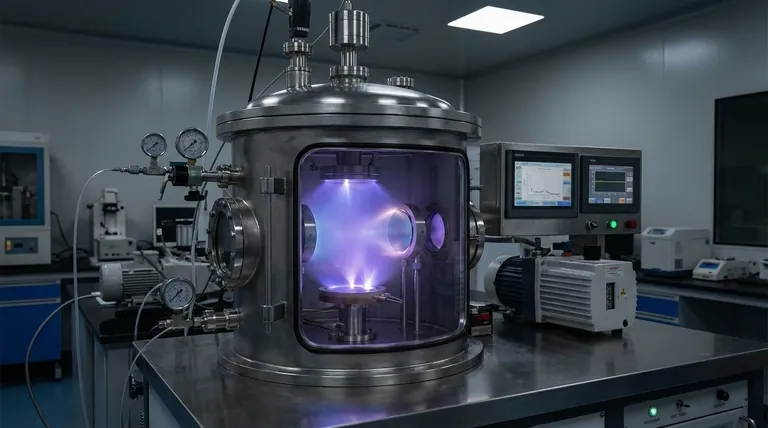
At its core, sputtering is a physical vapor deposition (PVD) process used to create exceptionally thin, high-performance films. It works by bombarding a source material, known as a target, with energized ions in a vacuum. This impact physically knocks atoms loose from the target, which then travel and deposit onto a substrate—such as a silicon wafer or optical lens—to form the desired coating.
Sputtering is best understood not as a single method, but as a family of highly controllable techniques. Its key advantage lies in its ability to deposit dense, strongly adherent films from an unmatched variety of materials, including complex alloys and insulators that are difficult or impossible to deposit using other methods.
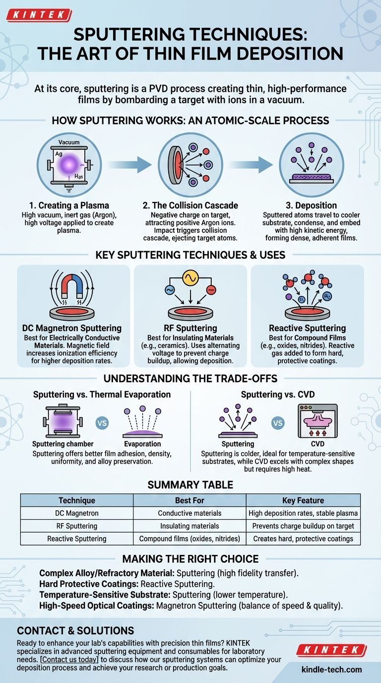
How Sputtering Works: An Atomic-Scale Process
Sputtering is a line-of-sight, mechanical process that functions on an atomic level. The mechanism can be broken down into three key stages.
The Core Mechanism: Creating a Plasma
The entire process occurs within a high-vacuum chamber. First, the chamber is evacuated, and then a small amount of an inert gas, typically Argon, is introduced.
A high voltage is applied, which ionizes the Argon gas and creates a glowing plasma—a superheated state of matter containing positive ions and free electrons.
The Collision Cascade: Ejecting Target Atoms
The target material (the source of the coating) is given a negative electrical charge. This attracts the positive Argon ions from the plasma, causing them to accelerate and strike the target surface with immense energy.
This bombardment triggers a collision cascade, similar to a cue ball breaking a rack of billiard balls. The impact's momentum is transferred through the target's atoms, ultimately causing surface atoms to be ejected, or "sputtered," from the target.
Deposition: Building the Thin Film
The sputtered atoms travel through the vacuum chamber and condense on the cooler surface of the substrate, which is strategically placed to intercept them.
Because these sputtered atoms have high kinetic energy, they embed themselves firmly into the substrate surface. This results in films that are typically much denser and have superior adhesion compared to films created by other methods like thermal evaporation.
Key Sputtering Techniques and Their Uses
The general sputtering principle can be adapted for different materials and outcomes, leading to several distinct techniques.
DC Magnetron Sputtering
This is one of the most common forms of sputtering, used for depositing electrically conductive materials. A magnetic field is applied behind the target to trap electrons near its surface, dramatically increasing the ionization efficiency of the Argon gas. This results in a more stable plasma and significantly higher deposition rates.
RF Sputtering
When the target material is an electrical insulator (like a ceramic), a direct current (DC) voltage causes positive charge to build up on its surface, eventually stopping the process. RF (Radio Frequency) sputtering solves this by using an alternating AC voltage, which alternately cleanses the charge buildup and allows the process to continue, enabling the deposition of insulating films.
Reactive Sputtering
In this technique, a reactive gas like oxygen or nitrogen is intentionally added to the vacuum chamber along with the inert Argon. The sputtered metal atoms react with this gas either in transit or on the substrate surface. This allows for the creation of compound films like oxides and nitrides, which are often used for hard, protective coatings on machine tools.
Understanding the Trade-offs
No single deposition technique is perfect for every job. Understanding sputtering's advantages and limitations is crucial for making an informed decision.
Sputtering vs. Thermal Evaporation
Thermal evaporation is another PVD technique where a material is heated until it vaporizes and condenses on a substrate. While often faster and simpler for pure metals, sputtering provides better film adhesion, density, and uniformity. Sputtering is also far superior for depositing alloys, as it largely preserves the composition of the target material in the final film.
Sputtering vs. Chemical Vapor Deposition (CVD)
CVD uses chemical reactions on a heated substrate to form a film. CVD can produce highly pure and conformal films that coat complex shapes very well. However, it requires very high temperatures, which can damage sensitive substrates like plastics or certain electronic components.
Sputtering is a "colder" physical process, making it ideal for temperature-sensitive substrates.
Common Limitations of Sputtering
Sputtering deposition rates can be lower than some thermal processes. The equipment is complex and represents a significant capital investment. Furthermore, because it is a line-of-sight process, achieving a uniform coating on complex, three-dimensional objects can be challenging without sophisticated substrate manipulation.
Making the Right Choice for Your Application
Selecting the correct deposition method depends entirely on the material properties, substrate, and desired outcome of your project.
- If your primary focus is depositing a complex alloy or refractory material: Sputtering is the superior choice because it transfers the target composition to the film with high fidelity.
- If your primary focus is creating hard, protective coatings for tools: Reactive sputtering is ideal for forming durable nitride, carbide, or oxide layers.
- If your primary focus is coating a temperature-sensitive substrate: Sputtering's lower process temperature gives it a distinct advantage over high-temperature CVD methods.
- If your primary focus is high-speed deposition of simple metals for optical coatings: Magnetron sputtering offers an excellent balance of speed, control, and film quality.
Ultimately, sputtering provides an unmatched level of control and material versatility for creating high-performance thin films.
Summary Table:
| Technique | Best For | Key Feature |
|---|---|---|
| DC Magnetron Sputtering | Conductive materials | High deposition rates, stable plasma |
| RF Sputtering | Insulating materials | Prevents charge buildup on target |
| Reactive Sputtering | Compound films (oxides, nitrides) | Creates hard, protective coatings |
Ready to enhance your lab's capabilities with precision thin films? KINTEK specializes in advanced sputtering equipment and consumables for laboratory needs. Whether you're working with sensitive substrates, complex alloys, or require hard protective coatings, our solutions deliver superior adhesion, density, and material versatility. Contact us today to discuss how our sputtering systems can optimize your deposition process and achieve your research or production goals.
Visual Guide
Related Products
- Chemical Vapor Deposition CVD Equipment System Chamber Slide PECVD Tube Furnace with Liquid Gasifier PECVD Machine
- Split Chamber CVD Tube Furnace with Vacuum Station Chemical Vapor Deposition System Equipment Machine
- Spark Plasma Sintering Furnace SPS Furnace
- RF PECVD System Radio Frequency Plasma-Enhanced Chemical Vapor Deposition RF PECVD
- Microwave Plasma Chemical Vapor Deposition MPCVD Machine System Reactor for Lab and Diamond Growth
People Also Ask
- What are the processes of vapor phase deposition? Understand CVD vs. PVD for Superior Thin Films
- What types of substrates are used in CVD to facilitate graphene films? Optimize Graphene Growth with the Right Catalyst
- What is the chemical vapor deposition growth process? Build Superior Thin Films from the Atom Up
- What happens during deposition chemistry? Building Thin Films from Gaseous Precursors
- What are the core advantages of PE-CVD in OLED encapsulation? Protect Sensitive Layers with Low-Temp Film Deposition


