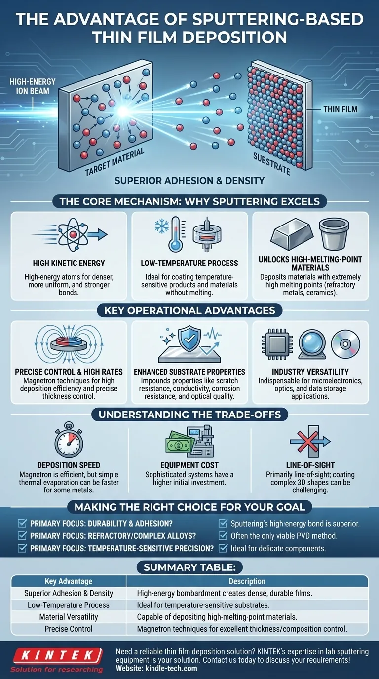
The primary advantage of sputtering is its ability to produce thin films with superior adhesion and density. Because the deposition process relies on high-energy physical bombardment rather than heat, it can be used on nearly any material—including those with extremely high melting points—and operates at lower temperatures, making it highly versatile and precise.
Sputtering excels because it is a high-energy physical vapor deposition (PVD) process. This energy translates directly into higher quality films that are denser, more uniform, and bonded more securely to the substrate than those produced by lower-energy methods like thermal evaporation.
The Core Mechanism: Why Sputtering Excels
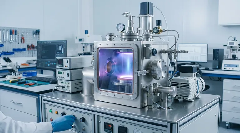
To understand the advantages of sputtering, it's essential to understand its physical nature. The process involves bombarding a target material with high-energy ions from a plasma, which physically ejects atoms that then deposit onto a substrate.
High Kinetic Energy for Superior Adhesion
The sputtered atoms travel from the target to the substrate with significantly higher kinetic energy than atoms from an evaporation process. This energy helps them form a denser, more uniform film and a stronger, more durable bond with the substrate surface.
A Purely Physical, Low-Temperature Process
Sputtering is a "dry" PVD process that does not involve liquids or complex chemical reactions. It also operates at much lower temperatures than methods like chemical vapor deposition (CVD), making it ideal for coating temperature-sensitive products or materials.
Unlocking High-Melting-Point Materials
Because sputtering does not require melting or evaporating the source material, it can deposit films from materials with very high melting points, such as refractory metals or certain ceramics. This is a critical advantage over thermal evaporation, which is limited by the material's boiling point.
Key Operational Advantages
Beyond the fundamental physics, sputtering provides several practical benefits that make it a cornerstone of modern manufacturing in industries from semiconductors to optics.
Precise Control and High Deposition Rates
Modern techniques like magnetron sputtering use powerful magnetic fields to confine the plasma near the target. This dramatically increases the efficiency of the sputtering process, leading to higher deposition rates and providing precise control over the film's thickness and composition.
Enhanced Substrate Properties
Sputtering is used not just to coat a surface but to fundamentally enhance it. The process can impart crucial properties such as improved scratch resistance, electrical conductivity, corrosion resistance, and optical qualities that the base material lacks.
Versatility Across Industries
The technique's reliability and material flexibility make it indispensable for a wide range of applications, including creating dielectric and nitride films in microelectronics, manufacturing hard drives and CDs, and producing advanced optical coatings.
Understanding the Trade-offs
While powerful, sputtering is not the universal solution for all thin-film needs. Being an effective advisor means acknowledging the context where other methods might be considered.
Deposition Speed vs. Other Methods
While magnetron sputtering is efficient, some simple thermal evaporation processes can be faster for depositing certain metals. The choice often depends on whether speed or ultimate film quality is the priority.
Equipment Complexity and Cost
Sputtering systems are sophisticated vacuum chambers that require high-voltage power supplies and gas management systems. This can make the initial equipment investment higher than that for simpler deposition techniques.
Line-of-Sight Limitations
Like many PVD processes, sputtering is primarily a line-of-sight technique. Coating complex, three-dimensional shapes with uniform thickness can be challenging and may require sophisticated substrate rotation and manipulation.
Making the Right Choice for Your Goal
Selecting the correct deposition method depends entirely on the desired outcome for your specific application.
- If your primary focus is film durability and adhesion: Sputtering's high-energy deposition creates a denser and more robust bond to the substrate, making it the superior choice.
- If your primary focus is depositing refractory or complex alloy materials: Sputtering is often the only viable PVD method for materials with extremely high melting points or for maintaining the stoichiometry of a complex target.
- If your primary focus is precision on temperature-sensitive substrates: Sputtering's low-temperature, highly controllable nature makes it ideal for delicate components like semiconductors, plastics, or optical elements.
Ultimately, sputtering provides a unique combination of material versatility, process control, and high-quality results that solves critical engineering challenges.
Summary Table:
| Key Advantage | Description |
|---|---|
| Superior Adhesion & Density | High-energy bombardment creates dense, durable films with excellent substrate bonding. |
| Low-Temperature Process | Ideal for temperature-sensitive substrates like plastics and semiconductors. |
| Material Versatility | Capable of depositing materials with extremely high melting points (e.g., refractory metals, ceramics). |
| Precise Control | Magnetron techniques allow for excellent control over film thickness and composition. |
Need a reliable thin film deposition solution for your lab?
Sputtering is a cornerstone technique for creating high-performance coatings in microelectronics, optics, and advanced materials research. If your project demands superior film adhesion, material versatility, or low-temperature processing, KINTEK's expertise in lab sputtering equipment is your solution.
We specialize in providing the precise, high-quality lab equipment and consumables you need to achieve your research and production goals. Let our experts help you select the ideal system for your specific application.
Contact KINTEL today to discuss your thin film deposition requirements and enhance your laboratory's capabilities!
Visual Guide
Related Products
- Aluminized Ceramic Evaporation Boat for Thin Film Deposition
- Tungsten Evaporation Boat for Thin Film Deposition
- Electron Beam Evaporation Coating Oxygen-Free Copper Crucible and Evaporation Boat
- Molybdenum Tungsten Tantalum Evaporation Boat for High Temperature Applications
- HFCVD Machine System Equipment for Drawing Die Nano-Diamond Coating
People Also Ask
- What is the chemical method for thin film deposition? Build Films from the Molecular Level Up
- Why is an alumina boat and Ti3AlC2 powder bed necessary for Ti2AlC sintering? Protect MAX Phase Purity
- What is the source of evaporation for thin film? Choosing Between Thermal and E-Beam Methods
- What is thin film deposition? Unlock Advanced Surface Engineering for Your Materials
- What are the alternatives to sputtering? Choose the Right Thin Film Deposition Method


