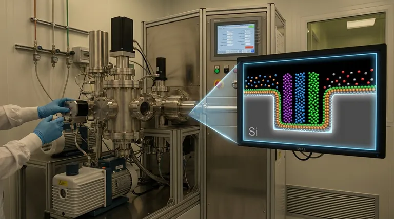
At its core, Atomic Layer Deposition (ALD) is a thin-film deposition technique used to create materials one single atomic layer at a time. It achieves this through a sequence of self-limiting chemical reactions. By repeating this sequence, or "cycle," you can build up a perfectly uniform film with precise, digital control over its final thickness.
The true power of ALD is not just about making things incredibly thin. It is about achieving unparalleled control, uniformity, and conformity over complex, three-dimensional surfaces where other deposition methods fail.
The ALD Cycle: A Step-by-Step Breakdown
To understand ALD, you must first grasp its foundational principle: the process is broken into a series of steps that are separated in time. This cyclic nature is what gives ALD its unique capabilities.
The Fundamental Principle: Self-Limiting Reactions
Each step in the ALD cycle is self-limiting. This means the chemical reaction stops on its own once all available reactive sites on the surface have been used. This prevents uncontrolled growth and is the key to achieving atomic-level precision.
Step 1: The First Precursor Pulse
The cycle begins by introducing the first chemical vapor, known as a precursor, into the reaction chamber. This precursor reacts with the surface until every available reactive site is occupied. Once the surface is saturated, the reaction naturally stops.
Step 2: The Purge
After the first reaction completes, the chamber is purged with an inert gas, such as nitrogen or argon. This purge completely removes any excess precursor molecules and gaseous byproducts, ensuring a clean surface for the next step.
Step 3: The Second Precursor (Reactant) Pulse
Next, a second precursor, often called the reactant (like water or oxygen plasma), is pulsed into the chamber. This chemical reacts with the first layer that was just deposited on the surface, completing the formation of a single, solid atomic layer of the desired material. This reaction is also self-limiting.
Step 4: The Final Purge
A final purge with inert gas removes all remaining reactant and byproducts from the chamber. This step leaves behind a pristine surface coated with a single, perfectly formed atomic layer of the target material.
The Result: A Single, Perfect Layer
At the end of these four steps, one ALD cycle is complete. The result is a single, uniform, and highly conformal layer of material. To grow a thicker film, you simply repeat the entire cycle until the desired thickness is achieved.
Why ALD is a Critical Manufacturing Technology
The unique, cyclic nature of ALD provides benefits that are essential for manufacturing modern, high-performance devices.
Unmatched Conformality
Conformality is the ability of a film to uniformly coat a surface, including complex 3D topographies like deep trenches or porous structures. Because ALD reactions occur everywhere on the surface, the technique can deposit a perfectly uniform film even on extremely high-aspect-ratio features, something impossible for most other methods.
Atomic-Level Thickness Control
The thickness of an ALD film is determined simply by the number of cycles performed. If one cycle deposits 0.1 nanometers of material, 100 cycles will deposit exactly 10 nanometers. This gives engineers a digital, highly repeatable method for controlling film thickness with atomic precision.
Exceptional Film Quality
ALD processes can often be run at lower temperatures than competing techniques like Chemical Vapor Deposition (CVD). This, combined with the precise, self-limiting reactions, results in films that are incredibly dense, pure, and have very few defects.
Understanding the Trade-offs
No technology is perfect, and ALD's precision comes at a cost. Understanding its limitations is critical for making informed decisions.
The Primary Limitation: Speed
The main drawback of ALD is its slow deposition rate. Because it builds material one atomic layer at a time, creating thick films can be extremely time-consuming and therefore expensive compared to faster, "bulk" deposition methods.
Precursor Chemistry and Cost
Developing a successful ALD process requires finding the right pair of precursor chemicals that react in a self-limiting manner. These chemicals can be complex, expensive, and sometimes difficult to handle safely, adding to the overall cost and complexity.
Equipment Complexity
ALD reactors are sophisticated instruments that require precise control over gas delivery, temperature, and pressure. The capital investment for this equipment is significant, making it best suited for high-value applications where its benefits are indispensable.
When to Consider Atomic Layer Deposition
Deciding whether ALD is the right choice depends entirely on your technical requirements and constraints.
- If your primary focus is ultimate precision and conformity: For applications like advanced semiconductor gate dielectrics, MEMS devices, or coating the inside of porous materials, ALD is often the only viable option.
- If your primary focus is coating simple, flat surfaces quickly: Traditional methods like Physical Vapor Deposition (PVD) or Chemical Vapor Deposition (CVD) are almost always more cost-effective and practical.
- If your primary focus is high-quality protective barriers: For applications like encapsulation of OLEDs or medical devices, the pinhole-free nature of ALD films makes it a superior choice, despite its lower speed.
Understanding the core mechanism of ALD empowers you to recognize the applications where its unique, layer-by-layer control is not just a benefit, but a fundamental necessity.
Summary Table:
| Key Aspect | Description |
|---|---|
| Core Principle | Self-limiting chemical reactions for atomic-level control. |
| Process | Cyclic steps: Precursor A, Purge, Precursor B, Purge. |
| Primary Advantage | Unmatched conformality on complex 3D surfaces. |
| Main Limitation | Slow deposition rate compared to other methods. |
Ready to harness the power of atomic-level precision for your lab?
KINTEK specializes in providing advanced lab equipment and consumables for cutting-edge research and development. If your project requires the unparalleled uniformity and conformality of Atomic Layer Deposition, our experts can help you identify the right solutions to meet your specific laboratory needs.
Contact us today via our form to discuss how our solutions can enhance your thin-film processes and drive your innovations forward.
Visual Guide

Related Products
- RF PECVD System Radio Frequency Plasma-Enhanced Chemical Vapor Deposition RF PECVD
- Chemical Vapor Deposition CVD Equipment System Chamber Slide PECVD Tube Furnace with Liquid Gasifier PECVD Machine
- HFCVD Machine System Equipment for Drawing Die Nano-Diamond Coating
- Customer Made Versatile CVD Tube Furnace Chemical Vapor Deposition Chamber System Equipment
- 915MHz MPCVD Diamond Machine Microwave Plasma Chemical Vapor Deposition System Reactor
People Also Ask
- How does plasma enhance CVD? Unlock Low-Temperature, High-Quality Film Deposition
- What is plasma enhanced chemical Vapour deposition process used for fabrication of? A Guide to Low-Temperature Thin Films
- What is plasma enhanced chemical vapour deposition PECVD used for? Enable Low-Temp Thin Films for Electronics & Solar
- What is an example of PECVD? RF-PECVD for High-Quality Thin Film Deposition
- What is plasma chemical vapor deposition? A Low-Temperature Thin Film Coating Solution


