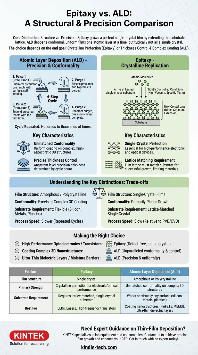
At its core, the difference between epitaxy and Atomic Layer Deposition (ALD) is a matter of structure versus precision. Epitaxy is a process designed to grow a perfect single-crystal film on top of a crystalline substrate, extending its atomic lattice. In contrast, ALD is a technique for depositing an exceptionally uniform and conformal thin film over any surface, with control down to a single atomic layer, but the resulting film is typically not a single crystal.
The choice between epitaxy and ALD is not about which is "better," but about your end goal. Choose epitaxy when the crystalline perfection of the film is critical for its electronic or optical function. Choose ALD when absolute thickness control and perfect coating of complex 3D shapes are the primary requirements.
What is Atomic Layer Deposition (ALD)?
ALD is an advanced deposition technique that builds films one atomic layer at a time. It belongs to the family of chemical vapor deposition (CVD) methods but offers significantly greater control.
The Principle of Self-Limiting Reactions
The ALD process operates in a cycle of four distinct steps:
- Pulse: A first chemical precursor gas is introduced into the chamber and reacts with the substrate surface.
- Purge: Excess precursor and byproducts are purged from the chamber with an inert gas. This reaction is self-limiting, meaning it stops once all available reaction sites on the surface are occupied.
- Pulse: A second precursor is introduced, which reacts only with the first precursor layer.
- Purge: The chamber is purged again, completing a single atomic layer.
This cycle is repeated hundreds or thousands of times to achieve the desired film thickness.
Key Characteristic: Unmatched Conformality
Because the chemical reactions occur on every exposed surface, ALD provides perfect conformality. It can uniformly coat extremely complex, high-aspect-ratio 3D structures, like deep trenches in a microchip, without any thinning at the bottom or corners.
Key Characteristic: Precise Thickness Control
Since the film is built one monolayer at a time, ALD offers angstrom-level precision. The final thickness is simply determined by the number of cycles performed, making it an exceptionally accurate and repeatable process.
What is Epitaxy?
Epitaxy is not just about depositing a film; it's about growing a new crystal layer that is a direct structural extension of the underlying crystalline substrate. The goal is to create a film with minimal defects and a perfectly ordered atomic structure.
The Principle of Crystalline Replication
In an epitaxy process, such as Molecular Beam Epitaxy (MBE) or Metalorganic Chemical Vapor Deposition (MOCVD), atoms or molecules arrive at a heated, single-crystal substrate surface. Under tightly controlled conditions (high vacuum, specific temperatures), these atoms have enough energy to move around and find their place in the crystal lattice, continuing the pattern of the substrate below.
Key Characteristic: Single-Crystal Perfection
The primary output of epitaxy is a single-crystal thin film. This level of atomic order is essential for high-performance semiconductor devices, such as lasers, LEDs, and high-frequency transistors, where crystal defects would degrade or destroy the device's performance.
Key Characteristic: The Lattice Matching Requirement
For successful epitaxy, the crystal lattice of the film being grown must be very similar in size and structure to the substrate's lattice. This constraint, known as lattice matching, is a critical requirement and limits the combinations of materials that can be used.
Understanding the Key Distinctions
The decision to use ALD or epitaxy comes down to a clear set of trade-offs tied directly to the intended application.
Film Structure: Crystalline vs. Amorphous/Polycrystalline
This is the most fundamental difference. Epitaxy produces single-crystal films. ALD typically produces amorphous (disordered) or polycrystalline (composed of many small crystal grains) films. While some forms of atomic layer epitaxy exist, standard ALD is not used for creating single-crystal layers.
Conformality: 3D Coating vs. Planar Growth
ALD excels at coating complex 3D topography with perfect uniformity. Epitaxy is primarily used for growing high-quality films on flat, planar substrates and is not designed to conformally coat complex shapes.
Substrate Requirements: Specific vs. General
Epitaxy demands a clean, single-crystal substrate that is lattice-matched to the film material. ALD is far more flexible and can be used to deposit films on almost any material, including silicon, metals, plastics, and powders.
Process Speed: Slow vs. Slower
Both processes are relatively slow compared to other deposition techniques like PVD or standard CVD. However, ALD is generally considered slower than epitaxy because of the repeated pulse-purge cycles required for each atomic layer.
Making the Right Choice for Your Application
Your goal dictates the correct technology. Analyze your primary requirement to select the right process.
- If your primary focus is high-performance optoelectronics (LEDs, lasers) or high-frequency transistors (HEMTs): You require the defect-free, single-crystal structure that only epitaxy can provide.
- If your primary focus is coating complex 3D nanostructures (like FinFETs in logic chips or MEMS devices): You need the unparalleled conformality and thickness control of ALD.
- If your primary focus is creating ultra-thin, pinhole-free dielectric layers (gate oxides) or moisture barriers: ALD's precision and uniformity are the superior choice.
Understanding the fundamental difference in mechanism and crystalline outcome is the key to selecting the right tool for your engineering challenge.
Summary Table:
| Feature | Epitaxy | Atomic Layer Deposition (ALD) |
|---|---|---|
| Film Structure | Single-crystal | Amorphous or Polycrystalline |
| Primary Strength | Crystalline perfection for electronic/optical performance | Unmatched conformality on complex 3D structures |
| Substrate Requirement | Requires lattice-matched, single-crystal substrate | Works on virtually any surface (silicon, metals, plastics, powders) |
| Best For | LEDs, Lasers, High-frequency transistors | Coating nanostructures (FinFETs, MEMS), ultra-thin dielectric layers |
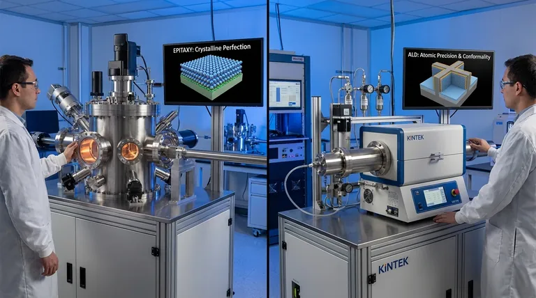
Need Expert Guidance on Thin-Film Deposition?
Choosing between epitaxy and ALD is critical for your project's success. The right equipment ensures optimal performance, whether you require single-crystal perfection for advanced semiconductors or atomic-level precision for complex 3D coatings.
KINTEK specializes in lab equipment and consumables, serving all your laboratory needs. We provide the tools and expertise to help you:
- Achieve precise film growth with reliable deposition systems.
- Enhance your R&D and production with equipment tailored to your specific application.
- Ensure repeatable results with high-quality consumables and expert support.
Contact us today to discuss your requirements and discover how KINTEK can support your thin-film deposition challenges. Get in touch via our contact form to speak with an expert!
Visual Guide