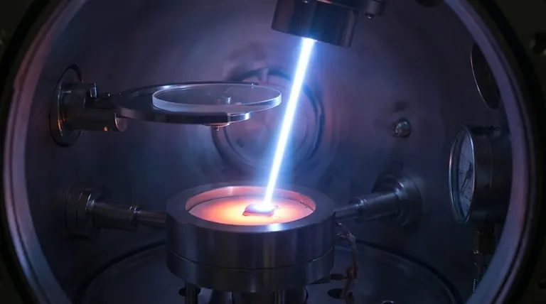
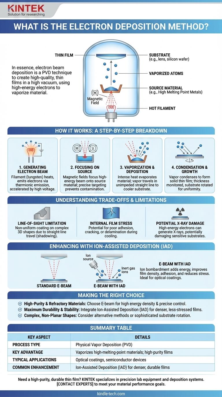
In essence, electron beam deposition is a physical vapor deposition (PVD) technique used to create high-quality, thin films of material. It operates in a high vacuum, using a focused beam of high-energy electrons to vaporize a source material. This resulting vapor then travels and condenses onto a target substrate, forming a precisely controlled coating.
The core principle of electron beam deposition is its ability to transfer immense energy into a small area. This allows it to vaporize even materials with very high melting points, producing exceptionally pure and well-controlled thin films that are critical for advanced applications like optics and electronics.
How Electron Beam Deposition Works: A Step-by-Step Breakdown
To truly understand this method, it's best to break it down into its core operational stages. The entire process takes place within a high-vacuum chamber to ensure the purity of the final film.
Stage 1: Generating the Electron Beam
An electron beam is generated from a hot filament, typically made of tungsten. This filament is heated to a point where it emits a cloud of electrons through a process called thermionic emission.
These free electrons are then accelerated by a strong electric field, which directs them with high voltage (typically several kilovolts) toward the source material.
Stage 2: Focusing on the Source Material
The beam of high-energy electrons is guided and focused using magnetic fields. This precision allows the beam to strike a very small spot on the source material, which is held in a water-cooled copper crucible or "hearth."
This targeted heating is a key advantage. It ensures that only the source material is vaporized, preventing contamination from the crucible itself.
Stage 3: Vaporization and Deposition
The intense, focused energy from the electron beam rapidly heats the source material to its boiling point, causing it to evaporate (or sublimate).
Because the chamber is under a high vacuum, the vaporized atoms travel in a straight, unimpeded line—a "line-of-sight" path—until they strike the cooler substrate (such as a lens, silicon wafer, or other component).
Stage 4: Condensation and Film Growth
Upon hitting the substrate, the vapor atoms condense and form a solid, thin film. The thickness of this film is monitored in real-time and controlled by adjusting the power of the electron beam, which dictates the rate of evaporation.
Substrates are often rotated to ensure the coating is applied as uniformly as possible across their surface.
Understanding the Trade-offs and Limitations
While powerful, electron beam deposition is not without its specific characteristics and potential challenges. Understanding these is critical for its successful application.
The Line-of-Sight Limitation
The straight-line path of the vaporized material means that it can be difficult to uniformly coat complex, three-dimensional shapes. Areas not in the direct line-of-sight of the source will receive little to no coating, a phenomenon known as "shadowing."
Internal Film Stress
Films deposited via E-beam can sometimes develop internal stress as they cool and solidify. This stress can lead to poor adhesion, cracking, or delamination if not properly managed.
Potential for X-ray Damage
The bombardment of a target with high-energy electrons can generate X-rays as a byproduct. While typically low-level, this radiation can potentially damage highly sensitive substrates, such as certain electronic components or polymers.
Enhancing the Process: Ion-Assisted Deposition (IAD)
To overcome some of these limitations, the E-beam process is often enhanced with a secondary technique called Ion-Assisted Deposition (IAD).
What is IAD?
During IAD, a separate ion source bombards the substrate with a low-energy beam of inert gas ions (like argon) while the vaporized material is depositing.
The Benefits of Ion Bombardment
This concurrent ion bombardment adds energy to the condensing atoms. This helps them arrange into a tighter, more ordered structure.
The result is a denser and more robust coating with significantly improved adhesion and lower internal stress. For high-performance optical coatings, IAD is often considered a standard requirement.
Making the Right Choice for Your Goal
Selecting a deposition method depends entirely on the material requirements and the application's end goal.
- If your primary focus is high-purity coatings or refractory materials: E-beam is an excellent choice due to its high energy density, material efficiency, and precise rate control.
- If your goal is maximum durability and environmental stability: Ensure the E-beam process is coupled with Ion-Assisted Deposition (IAD) to produce denser, less-stressed films.
- If you need to coat complex, non-planar shapes uniformly: You may need to consider alternative methods like sputtering, or ensure your E-beam system uses sophisticated substrate rotation.
By understanding these core principles, you can effectively specify the right deposition technique to achieve your material performance goals.
Summary Table:
| Key Aspect | Details |
|---|---|
| Process Type | Physical Vapor Deposition (PVD) |
| Key Advantage | Vaporizes high-melting-point materials; high-purity films |
| Typical Applications | Optical coatings, semiconductor devices |
| Common Enhancement | Ion-Assisted Deposition (IAD) for denser, more durable films |
Need a high-purity, durable thin film for your project?
KINTEK specializes in precision lab equipment, including advanced deposition systems. Our expertise ensures you get the right solution for coating high-performance optics, semiconductors, and other critical components.
Contact our experts today to discuss how our electron beam deposition technology can meet your specific material performance goals.
Visual Guide
Related Products
- Electron Beam Evaporation Coating Oxygen-Free Copper Crucible and Evaporation Boat
- RF PECVD System Radio Frequency Plasma-Enhanced Chemical Vapor Deposition RF PECVD
- Electron Beam Evaporation Coating Tungsten Crucible and Molybdenum Crucible for High Temperature Applications
- Electron Beam Evaporation Coating Conductive Boron Nitride Crucible BN Crucible
- Electron Beam Evaporation Coating Gold Plating Tungsten Molybdenum Crucible for Evaporation
People Also Ask
- How is an electron beam evaporator cooled during deposition? Essential Thermal Management for Stable Processes
- What is the deposition rate of e-beam evaporation? Control Thin Film Quality and Speed
- What is the current of e-beam evaporation? A Guide to High-Purity Thin Film Deposition
- What are the applications of electron beams? From Nanoscale Imaging to Industrial Manufacturing
- What is the container that holds the metal source material called in e-beam evaporation? Ensure Purity and Quality in Your Thin-Film Deposition


