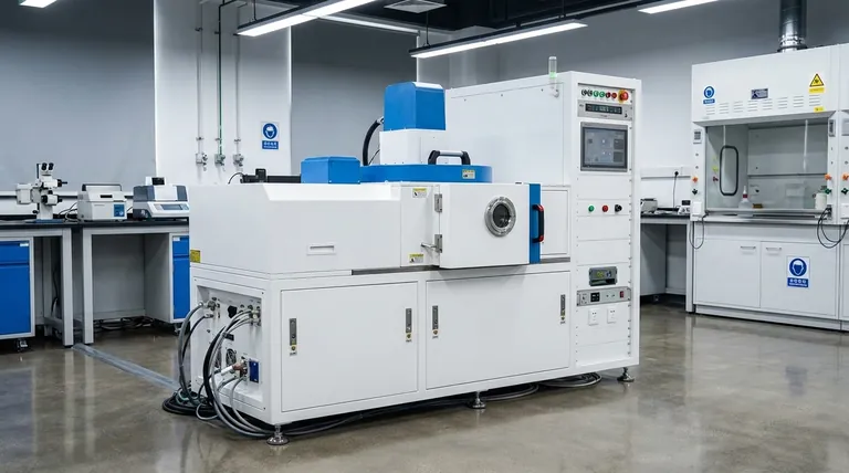
In short, physical deposition is a category of techniques used to create ultra-thin films of a solid material onto a surface, known as a substrate. These methods use physical means—such as heat or electromechanical force—to transfer atoms or molecules from a source material to the substrate inside a vacuum chamber, without any chemical reactions.
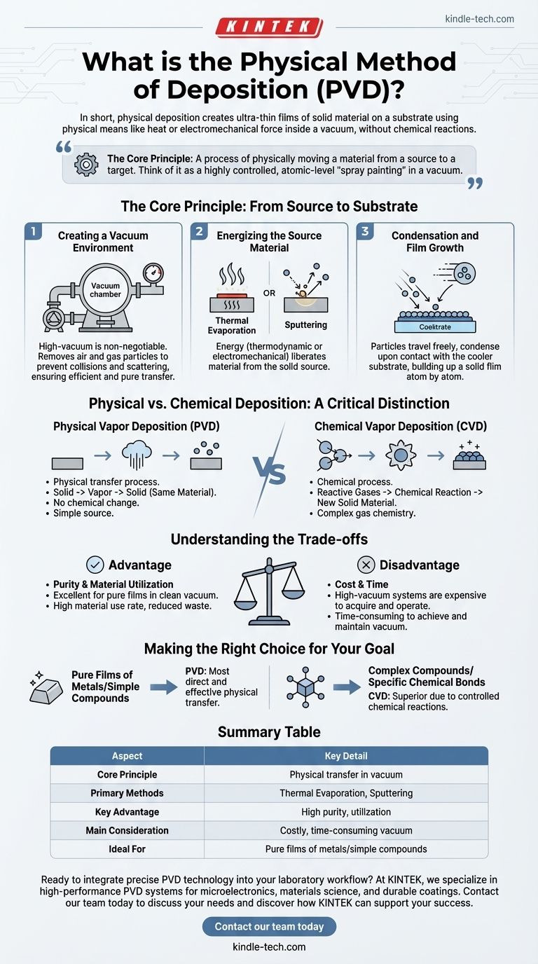
The core principle of physical deposition is straightforward: it's a process of physically moving a material from a source to a target. Think of it as a highly controlled, atomic-level "spray painting" where the "paint" is the source material turned into a vapor and the "canvas" is the substrate you wish to coat.
The Core Principle: From Source to Substrate
Physical Vapor Deposition (PVD), the primary class of physical deposition, is a line-of-sight process that relies on three fundamental steps to function. Each step is critical for forming a high-quality, uniform thin film.
Creating a Vacuum Environment
The entire process must occur in a high-vacuum chamber. This is non-negotiable.
The vacuum removes air and other gas particles that would otherwise collide with and scatter the vaporized material, preventing it from reaching the substrate efficiently and purely.
Energizing the Source Material
To move the material, it must first be liberated from its solid source.
This is accomplished by adding a significant amount of energy, typically through thermodynamic or electromechanical means. The two most common methods are thermal evaporation, which involves heating the material until it turns into a vapor, and sputtering, which uses energetic ions to knock atoms off the source.
Condensation and Film Growth
Once the particles of material are traveling freely through the vacuum, they reach the cooler substrate.
Upon contact, they condense back into a solid state, gradually building up on the surface atom by atom to form a thin, solid film.
Physical vs. Chemical Deposition: A Critical Distinction
Deposition technologies are broadly divided into two families: physical (PVD) and chemical (CVD). Understanding their fundamental difference is key to understanding the process.
The Defining Difference
Physical Vapor Deposition (PVD) is a physical transfer process. Material starts as a solid, is turned into a vapor, and lands on the substrate as the same solid material. No chemical change occurs.
Chemical Vapor Deposition (CVD) is a chemical process. It introduces reactive precursor gases into a chamber, which then react and decompose on the substrate's surface to form an entirely new solid material.
Simplicity of the Source
PVD is often considered a simpler process because it doesn't require complex or hazardous precursor gases. The source is simply the solid material you wish to deposit.
CVD, by contrast, relies on carefully controlled gas chemistry to produce the desired film.
Understanding the Trade-offs
While powerful, physical deposition methods are not a universal solution. The choice to use PVD involves clear advantages and disadvantages.
Advantage: Purity and Material Utilization
Because it is a direct physical transfer in a clean vacuum environment, PVD is excellent for creating very pure films.
It also offers a high material utilization rate, meaning more of the source material successfully ends up on the substrate, reducing waste.
Disadvantage: Cost and Time
The primary drawback of PVD is the need for a high-vacuum system.
These systems are expensive to acquire and operate. Achieving and maintaining the necessary vacuum is also time-consuming, which can make the overall process slower than some chemical alternatives.
Making the Right Choice for Your Goal
Selecting a deposition method depends entirely on the material properties required for the final film and the constraints of your application.
- If your primary focus is depositing a pure film of a metal or simple compound: PVD is often the most direct and effective choice due to its physical transfer mechanism.
- If your primary focus is creating a complex compound or a film that requires specific chemical bonds to form: Chemical Vapor Deposition (CVD) is likely the superior method because its process is based on controlled chemical reactions.
Ultimately, physical deposition is a foundational technology in modern manufacturing, enabling the creation of high-performance coatings that are essential for everything from microelectronics to durable consumer goods.
Summary Table:
| Aspect | Key Detail |
|---|---|
| Core Principle | Physical transfer of material from a solid source to a substrate in a vacuum. |
| Primary Methods | Thermal Evaporation, Sputtering. |
| Key Advantage | High material purity and utilization. |
| Main Consideration | Requires a high-vacuum environment, which can be costly and time-consuming. |
| Ideal For | Depositing pure films of metals and simple compounds. |
Ready to integrate precise PVD technology into your laboratory workflow?
At KINTEK, we specialize in high-performance lab equipment, including advanced PVD systems designed for reliability and superior thin-film results. Whether your focus is on microelectronics, materials science, or creating durable coatings, our experts can help you select the right solution to enhance your research and development.
Contact our team today to discuss your specific deposition needs and discover how KINTEK can support your laboratory's success.
Visual Guide
Related Products
- RF PECVD System Radio Frequency Plasma-Enhanced Chemical Vapor Deposition RF PECVD
- Chemical Vapor Deposition CVD Equipment System Chamber Slide PECVD Tube Furnace with Liquid Gasifier PECVD Machine
- 915MHz MPCVD Diamond Machine Microwave Plasma Chemical Vapor Deposition System Reactor
- Custom CVD Diamond Coating for Lab Applications
- Inclined Rotary Plasma Enhanced Chemical Vapor Deposition PECVD Equipment Tube Furnace Machine
People Also Ask
- What is plasma CVD? Unlock Low-Temperature Thin Film Deposition for Sensitive Materials
- What is plasma enhanced chemical Vapour deposition process used for fabrication of? A Guide to Low-Temperature Thin Films
- How does plasma enhance CVD? Unlock Low-Temperature, High-Quality Film Deposition
- What is plasma enhanced chemical vapour deposition PECVD used for? Enable Low-Temp Thin Films for Electronics & Solar
- What is an example of PECVD? RF-PECVD for High-Quality Thin Film Deposition


