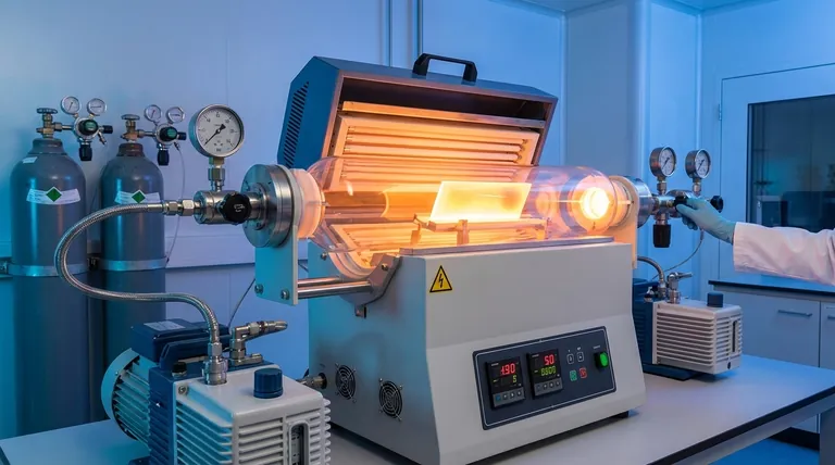
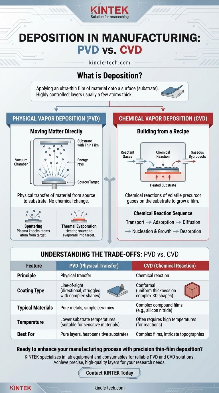
In manufacturing, deposition is the process of applying an ultra-thin film of material onto a surface, known as a substrate. This is a highly controlled technique used to build up layers often no thicker than a few atoms or molecules. The entire field is broadly divided into two main categories: Physical Vapor Deposition (PVD), which physically transfers material from a source to the substrate, and Chemical Vapor Deposition (CVD), which uses chemical reactions to grow a film directly on the substrate.
The core principle of deposition is not simply coating a surface, but rather constructing a new layer with precise properties at the atomic level. The fundamental choice is whether to physically move existing material onto the substrate (PVD) or to use a chemical recipe to build a new material there (CVD).
Physical Vapor Deposition (PVD): Moving Matter Directly
Physical Vapor Deposition encompasses a family of techniques where a solid or liquid source material is converted into a vapor and transported through a vacuum or low-pressure environment to condense on the substrate. The material being deposited does not undergo a chemical change.
The Core Principle: A Physical Transfer
Think of PVD as a highly controlled form of spray painting, but with individual atoms or molecules. A source material, or "target," is bombarded with energy, causing it to vaporize. These vaporized particles then travel in a straight line through a vacuum chamber and stick to the substrate, forming a solid thin film.
Example 1: Sputtering
In sputtering, the process begins by creating a high vacuum in a chamber to remove contaminants. A sputtering gas, often Argon, is introduced to create a plasma. This plasma bombards the source material (the target), physically knocking atoms off its surface. These dislodged atoms then travel and deposit onto the substrate.
Example 2: Thermal Evaporation
Thermal evaporation is one of the simplest PVD methods. A source material is heated in a high-vacuum chamber until it reaches a temperature where it begins to evaporate. This vapor stream travels through the vacuum and condenses on the cooler substrate, forming the desired film.
Chemical Vapor Deposition (CVD): Building from a Recipe
Chemical Vapor Deposition is fundamentally different. Instead of physically moving a material, CVD uses volatile precursor gases that react or decompose on the substrate's surface to create the thin film.
The Core Principle: A Chemical Transformation
Think of CVD as precisely "baking" a new layer onto a surface. One or more gases are introduced into a reaction chamber. When these gases reach the heated substrate, they undergo a chemical reaction that results in a solid product being deposited on the surface, while gaseous byproducts are removed.
The Chemical Reaction Sequence
The CVD process involves several distinct steps. First, the reactant gases are transported to the substrate surface. The species are then adsorbed, where they can diffuse across the surface to growth sites. Finally, catalyzed surface reactions lead to the nucleation and growth of the film, while gaseous byproducts are desorbed and transported away.
Understanding the Trade-offs: PVD vs. CVD
Choosing between these two methods depends entirely on the desired properties of the film and the nature of the substrate.
Material Purity and Complexity
PVD is ideal for depositing pure materials, such as metals or simple ceramics. Since you are just physically transferring the source material, the composition of the film is largely identical to the target.
CVD excels at creating complex compound films like silicon nitride or silicon dioxide. The process is designed to create these materials in-situ through controlled chemical reactions that would be difficult or impossible with PVD.
Conformal Coating vs. Line-of-Sight
PVD is a "line-of-sight" process. The vaporized material travels in a straight line, meaning it can effectively coat surfaces directly facing the source but struggles to coat complex, three-dimensional shapes or the sides of deep trenches.
CVD provides excellent "conformal" coating. Because the precursor gases can flow and react on all exposed surfaces, CVD can deposit a film of uniform thickness over intricate topographies, which is critical in microelectronics manufacturing.
Temperature and Substrate Sensitivity
CVD processes often require high substrate temperatures to drive the necessary chemical reactions. This can limit their use with materials that are sensitive to heat. Many PVD techniques can be performed at much lower temperatures, making them suitable for a wider range of substrates.
Making the Right Choice for Your Application
Your choice between PVD and CVD hinges entirely on your end goal for the final product.
- If your primary focus is applying a pure metal or simple ceramic layer: PVD is often the more direct, reliable, and cost-effective method.
- If your primary focus is creating a complex, high-purity compound film: CVD is necessary to build the material chemically on the substrate surface.
- If your primary focus is coating a complex, three-dimensional surface evenly: CVD's ability to create highly conformal layers is a significant advantage over line-of-sight PVD.
Understanding this fundamental divide between physical transfer and chemical creation is the key to mastering thin-film manufacturing.
Summary Table:
| Feature | Physical Vapor Deposition (PVD) | Chemical Vapor Deposition (CVD) |
|---|---|---|
| Principle | Physical transfer of material via vaporization | Chemical reaction of gases on substrate surface |
| Coating Type | Line-of-sight | Conformal (covers complex 3D shapes evenly) |
| Typical Materials | Pure metals, simple ceramics | Complex compounds (e.g., silicon nitride) |
| Temperature | Lower substrate temperatures | Often requires high temperatures |
| Best For | Pure layers, heat-sensitive substrates | Complex films, intricate topographies |
Ready to enhance your manufacturing process with precision thin-film deposition? KINTEK specializes in lab equipment and consumables for deposition applications, serving laboratories that require reliable PVD and CVD solutions. Whether you need to deposit pure metals with PVD or create complex compound films with CVD, our expertise ensures you achieve the precise, high-quality layers your products demand. Contact us today to discuss how our tailored deposition solutions can optimize your laboratory's efficiency and results!
Visual Guide
Related Products
- RF PECVD System Radio Frequency Plasma-Enhanced Chemical Vapor Deposition RF PECVD
- Evaporation Boat for Organic Matter
- Thin-Layer Spectral Electrolysis Electrochemical Cell
- Side Window Optical Electrolytic Electrochemical Cell
- Reference Electrode Calomel Silver Chloride Mercury Sulfate for Laboratory Use
People Also Ask
- What is plasma CVD? Unlock Low-Temperature Thin Film Deposition for Sensitive Materials
- What is plasma enhanced chemical vapour deposition process? Unlock Low-Temperature, High-Quality Thin Films
- What is plasma enhanced chemical Vapour deposition process used for fabrication of? A Guide to Low-Temperature Thin Films
- What is plasma enhanced chemical vapour deposition PECVD used for? Enable Low-Temp Thin Films for Electronics & Solar
- What is an example of PECVD? RF-PECVD for High-Quality Thin Film Deposition


