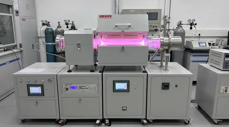
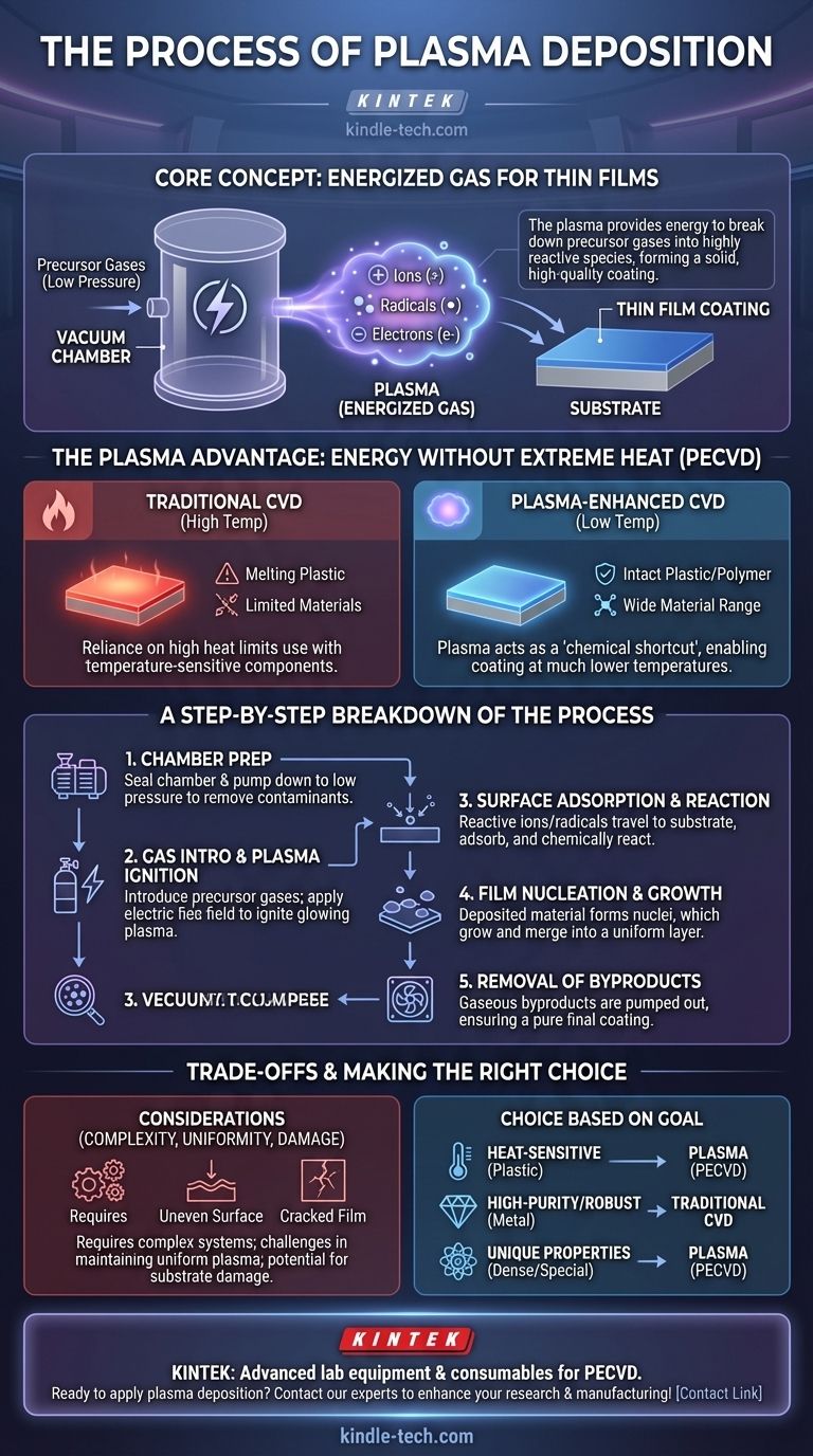
At its core, plasma deposition is a process that uses an energized gas, or plasma, to create the conditions necessary for a thin film to grow on a surface. Within a vacuum chamber, the plasma provides the energy to break down precursor gases into highly reactive chemical species. These reactive species then condense and form a solid, high-quality coating on a target object, known as a substrate.
The critical function of plasma in deposition is not to heat the entire chamber, but to energize the source gases directly. This "chemical shortcut" creates reactive particles that form a coating at much lower temperatures than traditional methods, dramatically expanding the range of materials that can be coated.
The Foundation: Why Plasma is Used
To understand plasma deposition, it's helpful to first understand the process it enhances: Chemical Vapor Deposition (CVD).
The Standard CVD Process
In a traditional CVD process, a substrate is placed in a reaction chamber and heated to very high temperatures.
Precursor gases containing the coating material are then introduced. The extreme heat provides the energy needed to break the chemical bonds in these gases, allowing them to react on the hot substrate surface and form the desired film.
The Limitation of Heat
The reliance on high temperatures is the primary limitation of standard CVD. It means you cannot coat materials with low melting points, such as plastics, certain polymers, or other temperature-sensitive components, without damaging or destroying them.
The Plasma Advantage: Energy Without Extreme Heat
Plasma-Enhanced Chemical Vapor Deposition (PECVD) overcomes this heat limitation by using plasma as the energy source.
Plasma Generation
An electrical field is applied to the low-pressure precursor gas inside the chamber. This energy strips electrons from the gas atoms or molecules, creating a mixture of free electrons, positively charged ions, and highly reactive neutral particles called radicals. This energized, ionized gas is the plasma.
Direct Gas Activation
This plasma environment is extremely energetic. The collisions within the plasma efficiently break down the stable precursor gases into the necessary reactive species.
This activation happens in the gas phase itself, not because the substrate is hot. The energy is delivered precisely where it's needed—to the precursor molecules.
The Low-Temperature Benefit
Because the plasma does the heavy lifting of breaking chemical bonds, the substrate does not need to be intensely heated. This allows for the deposition of high-quality, durable coatings on materials that would melt or deform in a traditional CVD reactor.
A Step-by-Step Breakdown of the Process
The plasma deposition process follows a series of carefully controlled steps to build the film layer by layer.
1. Chamber Preparation
The process begins by placing the substrate into a vacuum chamber. The chamber is sealed and pumped down to a very low pressure to remove air and any potential contaminants, such as dust or water vapor.
2. Gas Introduction and Plasma Ignition
The precursor gases, which contain the atoms for the desired film, are introduced into the chamber at a controlled flow rate. An electric field is then applied, igniting the gas and transforming it into a glowing plasma.
3. Surface Adsorption and Reaction
The ions and radicals created in the plasma diffuse and travel toward the substrate. These highly reactive particles stick to the surface (adsorption) and react with each other to form the solid film.
4. Film Nucleation and Growth
The deposited material begins to form small islands, or nuclei, on the substrate. As the process continues, these nuclei grow and merge, creating a continuous, uniform thin film across the entire surface.
5. Removal of Byproducts
Any gaseous byproducts from the chemical reactions are removed from the chamber by the vacuum pumping system, ensuring a clean process and a pure final coating.
Understanding the Trade-offs
While powerful, plasma deposition is not without its complexities.
System Complexity
PECVD systems are more complex and expensive than simple thermal CVD ovens. They require sophisticated power supplies, gas handling systems, and vacuum technology to generate and control the plasma.
Achieving Uniformity
Maintaining a perfectly uniform plasma over a large or complexly shaped substrate can be challenging. Non-uniform plasma can lead to variations in the thickness and properties of the final coating.
Potential for Damage
The high-energy particles within the plasma can sometimes cause unintended damage to the substrate surface or the growing film. This requires careful tuning of the plasma conditions to balance reactivity with control.
Making the Right Choice for Your Goal
Selecting the right deposition method depends entirely on your material and desired outcome.
- If your primary focus is coating heat-sensitive substrates like plastics or polymers: Plasma deposition is the superior choice because it enables high-quality film growth without damaging the underlying material.
- If your primary focus is achieving high-purity films on robust, high-temperature materials: Traditional, high-temperature CVD might be a simpler and more cost-effective solution.
- If your primary focus is creating dense films with unique properties: The energetic plasma environment can create films with structures and characteristics that are difficult to achieve with purely thermal methods.
Ultimately, plasma deposition provides a level of process control and material versatility that fundamentally expands the possibilities of surface engineering.
Summary Table:
| Process Step | Key Action | Outcome |
|---|---|---|
| Chamber Prep | Create vacuum | Remove contaminants |
| Plasma Ignition | Apply electric field to gas | Generate reactive ions/radicals |
| Surface Reaction | Particles adsorb to substrate | Film nucleation begins |
| Film Growth | Continuous deposition | Uniform thin film formation |
| Byproduct Removal | Vacuum pumping | Pure final coating |
Ready to apply plasma deposition technology in your lab? KINTEK specializes in advanced lab equipment and consumables for plasma-enhanced chemical vapor deposition (PECVD) processes. Whether you're working with temperature-sensitive polymers, plastics, or need precise thin-film coatings, our solutions help you achieve superior surface engineering results. Contact our experts today to discuss how our PECVD systems can enhance your research and manufacturing capabilities!
Visual Guide
Related Products
- RF PECVD System Radio Frequency Plasma-Enhanced Chemical Vapor Deposition RF PECVD
- Inclined Rotary Plasma Enhanced Chemical Vapor Deposition PECVD Equipment Tube Furnace Machine
- Inclined Rotary Plasma Enhanced Chemical Vapor Deposition PECVD Equipment Tube Furnace Machine
- Chemical Vapor Deposition CVD Equipment System Chamber Slide PECVD Tube Furnace with Liquid Gasifier PECVD Machine
- Microwave Plasma Chemical Vapor Deposition MPCVD Machine System Reactor for Lab and Diamond Growth
People Also Ask
- What is plasma chemical vapor deposition? A Low-Temperature Thin Film Coating Solution
- Why is a Matching Network Indispensable in RF-PECVD for Siloxane Films? Ensure Stable Plasma and Uniform Deposition
- How does plasma enhance CVD? Unlock Low-Temperature, High-Quality Film Deposition
- What is the role of RF-PECVD in VFG preparation? Mastering Vertical Growth and Surface Functionality
- How does Radio Frequency Enhanced Plasma Chemical Vapour Deposition (RF-PECVD) work? Learn the Core Principles


