In short, the process of thin film optical coating involves depositing one or more microscopic layers of specific materials onto an optical component, like a lens or mirror, inside a vacuum chamber. The exact method is chosen based on the material and the desired optical effect, but the fundamental principle is to build up a film, often just a few molecules thick, that precisely controls how light reflects, transmits, or is absorbed.
The core concept is not about a single method, but a family of highly controlled deposition techniques. The choice between them is a critical engineering decision, balancing the desired optical performance, film durability, and manufacturing cost.
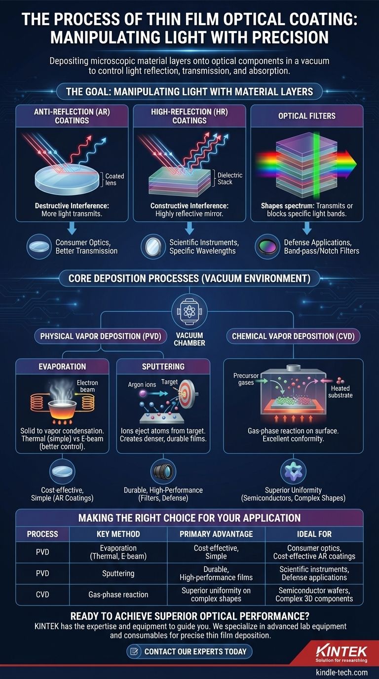
The Goal: Manipulating Light with Material Layers
Before diving into the "how," it's crucial to understand the "why." Optical coatings work by creating interference effects. When light hits the boundary between different materials (like air, the coating, and the glass), some of it reflects and some passes through. By precisely controlling the thickness and refractive index of the coating layer(s), we can control whether these reflected waves reinforce or cancel each other out.
Anti-Reflection (AR) Coatings
The most common application is an anti-reflection (AR) coating. A single layer with a carefully chosen thickness (one-quarter of the light's wavelength) and refractive index can cause the light reflecting from the top of the coating to be perfectly out of phase with the light reflecting from the bottom. This destructive interference causes the reflections to cancel each other out, allowing more light to transmit through the lens.
High-Reflection (HR) Coatings
Conversely, by stacking multiple alternating layers of high and low refractive index materials (a "dielectric stack"), we can create constructive interference. This causes reflections from each interface to reinforce one another, creating a highly reflective mirror for a specific range of wavelengths.
Optical Filters
This same principle allows for the creation of sophisticated optical filters. By carefully designing the stack of layers, we can create coatings that transmit only a very narrow band of light (band-pass filters) or block a specific range (notch filters), effectively shaping the spectrum of light passing through the component.
Core Deposition Processes
All modern optical coating happens in a vacuum to ensure purity and control. The primary methods fall into two major families: Physical Vapor Deposition (PVD) and Chemical Vapor Deposition (CVD).
Physical Vapor Deposition (PVD)
PVD involves turning a solid source material into a vapor, which then travels through the vacuum and condenses onto the cooler optical substrate, forming a thin film.
- Evaporation: This is the most established PVD method. The source material is heated in a crucible until it evaporates.
- Thermal Evaporation uses resistive heating (like a toaster coil) and is simpler but offers less control.
- Electron-Beam (E-beam) Evaporation uses a high-energy beam of electrons to heat the material, allowing for the deposition of materials with very high melting points and providing better rate control.
- Sputtering: In this process, a target made of the coating material is bombarded with high-energy ions (usually argon). These ions act like microscopic sand-blasters, knocking atoms off the target. These "sputtered" atoms then travel and deposit onto the substrate, creating a film that is typically denser and more durable than an evaporated film.
Chemical Vapor Deposition (CVD)
CVD is fundamentally different. Instead of physically vaporizing a solid, this process introduces precursor gases into the chamber. These gases react or decompose on the hot substrate surface, leaving behind the desired solid material as a thin film. CVD is excellent for creating highly uniform films that conform perfectly to complex shapes.
Understanding the Trade-offs
No single process is best for all applications. The choice involves critical engineering trade-offs.
Process vs. Performance
Sputtered films are generally denser, more durable, and more stable over time and with temperature changes compared to evaporated films. The higher energy of the sputtered atoms leads to a more robust film structure. However, sputtering equipment can be more complex and expensive.
Durability and Adhesion
Adding an ion source to assist the deposition process (known as Ion-Assisted Deposition, or IAD) can dramatically improve the density and adhesion of evaporated films. This bridges the performance gap between evaporation and sputtering, offering a good balance of quality and cost.
Material Limitations
Some complex chemical compounds can break down when heated for evaporation. For these materials, sputtering is often the only viable PVD method, as it ejects atoms from the target without melting the bulk material. CVD offers another path but requires finding suitable precursor gases and managing high substrate temperatures.
Making the Right Choice for Your Application
Selecting the correct process requires aligning the method's strengths with your primary goal.
- If your primary focus is cost-effective AR coatings for consumer optics: Standard thermal or e-beam evaporation is often the most economical and sufficient choice.
- If your primary focus is durable, high-performance filters for scientific or defense applications: Sputtering or ion-assisted deposition is necessary to achieve the required density and environmental stability.
- If your primary focus is coating complex 3D shapes or large-area semiconductor wafers uniformly: Chemical Vapor Deposition (CVD) is often the superior method due to its excellent conformity.
Ultimately, mastering these deposition processes is what enables the creation of everything from better camera lenses to advanced astronomical telescopes.
Summary Table:
| Deposition Process | Key Method | Primary Advantage | Ideal For |
|---|---|---|---|
| Physical Vapor Deposition (PVD) | Evaporation (Thermal, E-beam) | Cost-effective, simple | Consumer optics, cost-effective AR coatings |
| Physical Vapor Deposition (PVD) | Sputtering | Durable, high-performance films | Scientific instruments, defense applications |
| Chemical Vapor Deposition (CVD) | Gas-phase reaction | Superior uniformity on complex shapes | Semiconductor wafers, complex 3D components |
Ready to Achieve Superior Optical Performance?
Choosing the right thin film coating process is critical for your application's success. Whether you need durable, high-performance filters for scientific research or cost-effective AR coatings for consumer products, KINTEK has the expertise and equipment to guide you.
We specialize in providing advanced lab equipment and consumables for precise thin film deposition. Our solutions help you achieve the exact optical properties you need, from enhanced light transmission to superior durability.
Contact our experts today to discuss your specific requirements and discover how KINTEK can optimize your optical coating process.
Visual Guide
Related Products
- Chemical Vapor Deposition CVD Equipment System Chamber Slide PECVD Tube Furnace with Liquid Gasifier PECVD Machine
- RF PECVD System Radio Frequency Plasma-Enhanced Chemical Vapor Deposition RF PECVD
- HFCVD Machine System Equipment for Drawing Die Nano-Diamond Coating
- Microwave Plasma Chemical Vapor Deposition MPCVD Machine System Reactor for Lab and Diamond Growth
- Customer Made Versatile CVD Tube Furnace Chemical Vapor Deposition Chamber System Equipment
People Also Ask
- What happens during deposition chemistry? Building Thin Films from Gaseous Precursors
- How are carbon nanotubes grown? Master Scalable Production with Chemical Vapor Deposition
- What is plasma enhanced chemical vapor deposition PECVD equipment? A Guide to Low-Temperature Thin Film Deposition
- What types of substrates are used in CVD to facilitate graphene films? Optimize Graphene Growth with the Right Catalyst
- What are the advantages of chemical vapor deposition? Achieve Superior Thin Films for Your Lab