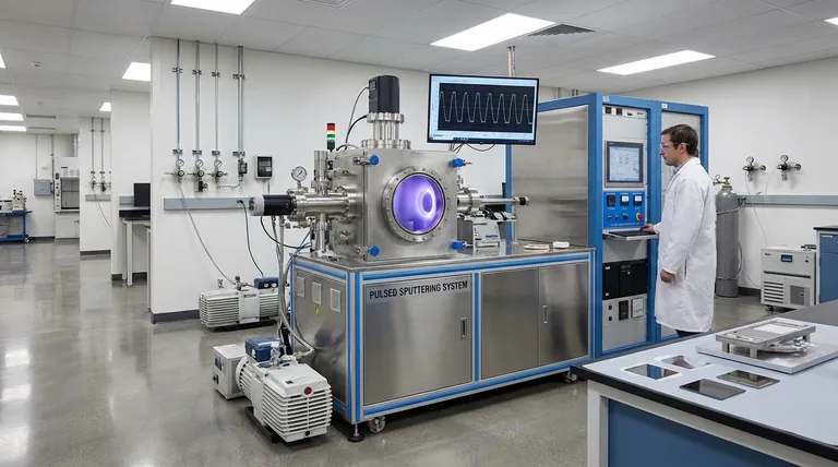
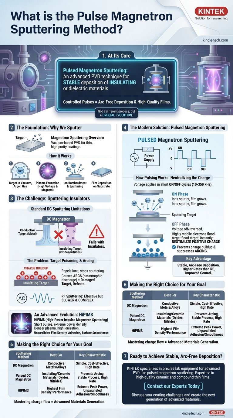
At its core, pulsed magnetron sputtering is an advanced physical vapor deposition (PVD) technique that solves a critical problem found in standard DC sputtering: the unstable deposition of insulating or dielectric materials. It works by applying power to the sputtering target in short, controlled pulses rather than as a continuous current. This pulsing mechanism prevents the destructive electrical arcs that would otherwise form on an insulating target, enabling the creation of high-quality ceramic and compound thin films with excellent stability and control.
Pulsed sputtering is not a fundamentally different process, but rather a crucial evolution. It combines the high deposition rates of DC sputtering with the material versatility of RF sputtering, offering a superior, modern solution for depositing high-performance insulating thin films.
The Foundation: Why We Sputter
Magnetron sputtering is a vacuum-based process used to deposit exceptionally thin, high-purity coatings onto a substrate. It is valued for its ability to create films with superior adhesion and uniformity compared to other methods like thermal evaporation.
How Magnetron Sputtering Works
The process begins with a solid slab of the coating material, known as the target. This target is placed in a vacuum chamber, which is then filled with an inert gas, typically Argon.
A high voltage is applied to the target, causing the gas to ionize and form a plasma. A powerful magnetic field behind the target traps electrons near its surface, dramatically increasing the efficiency of the ionization process.
Positively charged Argon ions are accelerated by the electric field and collide with the negatively charged target. These high-energy collisions physically knock out, or "sputter," atoms from the target material. These sputtered atoms then travel through the vacuum and deposit onto a substrate, building up a thin film layer by layer.
The Power of Sputtered Films
Atoms ejected from a sputtered target have significantly higher kinetic energy than those from an evaporated source. This high energy results in films that are denser and have much better adhesion to the substrate.
Furthermore, sputtering can deposit virtually any material, including alloys, compounds, and elements with extremely high melting points, all without needing to melt the source material.
The Challenge: Sputtering Insulating Materials
While standard DC (Direct Current) sputtering is highly effective for conductive metal targets, it fails when attempting to deposit electrically insulating materials like oxides or nitrides.
The Problem with DC: Target Poisoning and Arcing
In DC sputtering, the target is held at a constant negative voltage to attract the positive Argon ions. If the target is an insulator, these positive ions accumulate on its surface because the charge has nowhere to go.
This buildup of positive charge, sometimes called "target poisoning," eventually repels incoming Argon ions, slowing or stopping the sputtering process. Worse, it can lead to a sudden, catastrophic discharge of energy known as an arc, which can damage the target and blast debris into the growing film, creating defects.
The Traditional Solution: RF Sputtering
The classic solution to this problem was to use a Radio Frequency (RF) power supply instead of a DC one. The rapidly alternating AC voltage alternately attracts ions (to sputter) and then electrons (to neutralize the charge buildup).
While effective, RF sputtering has significant drawbacks. It generally has a much lower deposition rate than DC sputtering and requires complex, expensive power supplies with impedance matching networks, making the process less efficient and more difficult to control.
The Modern Solution: Pulsed Magnetron Sputtering
Pulsed sputtering was developed to overcome the limitations of both DC and RF methods, offering a robust and efficient way to deposit insulating films.
How Pulsing Works: Neutralizing the Charge
Instead of a continuous DC voltage, a pulsed power supply applies voltage in a series of short on/off cycles at a mid-range frequency (typically 10-350 kHz).
During the longer "on" phase, the target sputters just like in a DC process. During the very brief "off" phase, the voltage is either shut off or reversed to be slightly positive. This attracts a flood of highly mobile electrons from the plasma, which instantly neutralize the positive charge that accumulated on the target's surface.
The Key Advantage: Stable, Arc-Free Deposition
This simple on/off cycle effectively prevents charge buildup and suppresses arcing before it can begin. This leads to an extremely stable, repeatable process capable of producing high-quality, defect-free insulating films.
The deposition rates are typically much higher than RF sputtering, and the process control is significantly improved.
An Advanced Evolution: HiPIMS
A specialized form of this technique is High-Power Impulse Magnetron Sputtering (HiPIMS). HiPIMS uses very short pulses with extremely high peak power densities. This creates a much denser plasma with a high degree of ionization, resulting in sputtered films with unparalleled density, adhesion, and surface smoothness.
Making the Right Choice for Your Goal
Understanding the role of pulsing allows you to select the ideal sputtering technology for your specific application.
- If your primary focus is simple conductive films: Standard DC magnetron sputtering is the most straightforward and cost-effective method for depositing pure metals and conductive alloys.
- If your primary focus is depositing insulating or ceramic materials: Pulsed DC magnetron sputtering is the modern industry standard, providing high-rate, stable deposition of materials like oxides, nitrides, and other dielectrics.
- If your primary focus is achieving the highest possible film density and performance: HiPIMS is the superior, albeit more complex, technology for creating advanced coatings where structural perfection is paramount.
By mastering the flow of charge at the target surface, pulsed sputtering empowers engineers and scientists to create a new generation of advanced materials.
Summary Table:
| Sputtering Method | Best For | Key Characteristic |
|---|---|---|
| DC Magnetron | Conductive metals/alloys | Simple, cost-effective, high deposition rate |
| Pulsed DC Magnetron | Insulating/ceramic materials (oxides, nitrides) | Prevents arcing, stable process, high rate |
| HiPIMS | Highest film density/performance | Extreme peak power, unparalleled adhesion/smoothness |
Ready to achieve stable, arc-free deposition of your advanced insulating films?
KINTEK specializes in providing the precise lab equipment and consumables you need for advanced PVD processes like pulsed magnetron sputtering. Our expertise ensures you get the right solution for depositing high-quality ceramic and compound thin films with excellent control and stability.
Contact our experts today to discuss how we can support your laboratory's specific coating challenges and help you create the next generation of advanced materials.
Visual Guide
Related Products
- Spark Plasma Sintering Furnace SPS Furnace
- RF PECVD System Radio Frequency Plasma-Enhanced Chemical Vapor Deposition RF PECVD
People Also Ask
- What is SPS sintering method? A Guide to High-Speed, High-Performance Material Fabrication
- What is the pressure for spark plasma sintering? A Guide to Optimizing SPS Parameters
- What is the process fundamentals of spark plasma sintering? Achieve Rapid, High-Density Material Consolidation
- What technical advantages does a Spark Plasma Sintering (SPS) furnace offer for LZP ceramics? Enhance Ionic Conductivity
- Why are Spark Plasma Sintering (SPS) furnaces or hot presses utilized in the preparation of Li3PS4 solid electrolytes?

