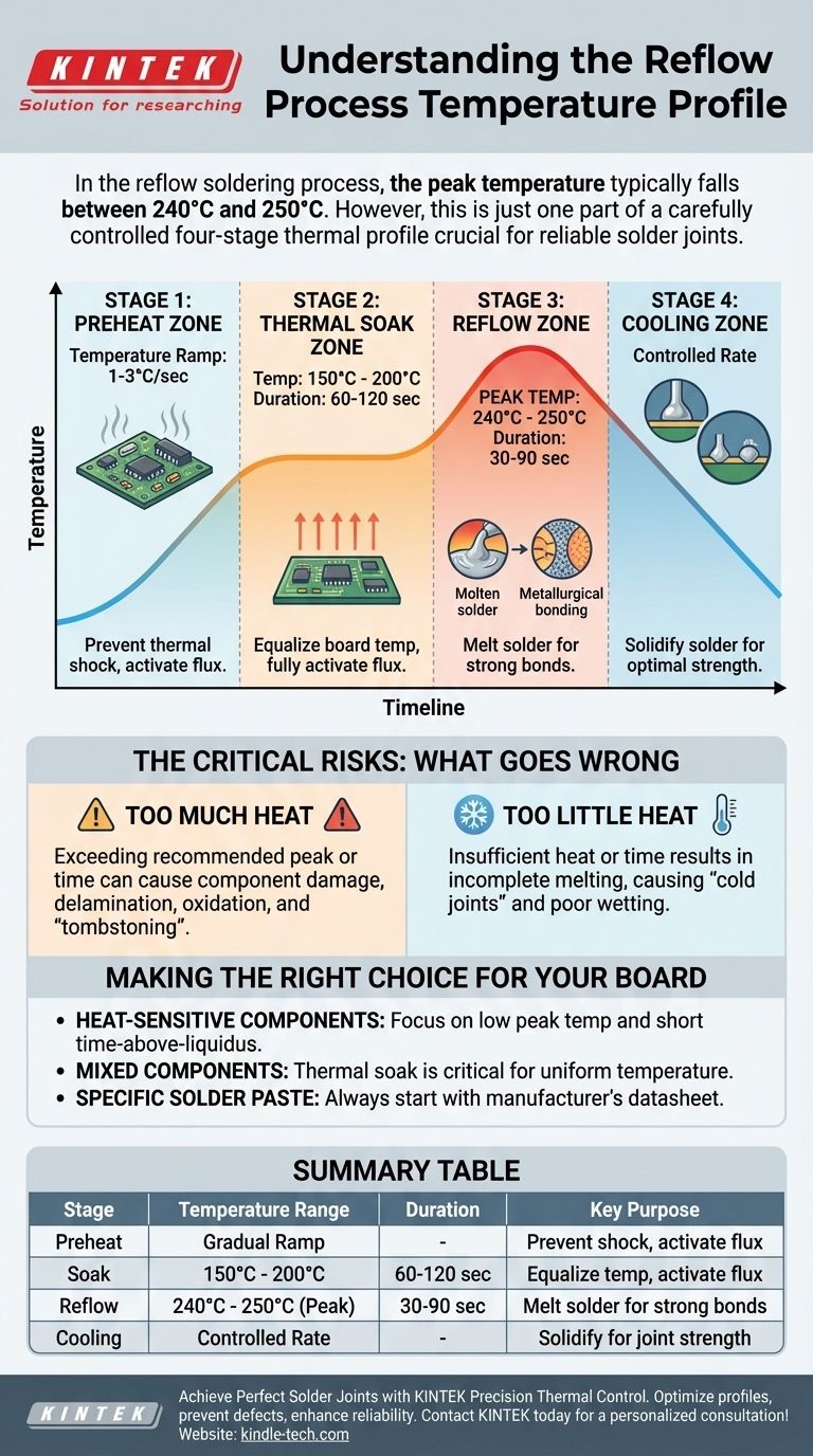
In the reflow soldering process, the peak temperature typically falls between 240°C and 250°C for common lead-free solder pastes. However, this peak temperature is only one part of a carefully controlled thermal sequence known as a reflow profile, which is essential for creating reliable solder joints without damaging components.
The key is to understand that "reflow temperature" is not a single value but a multi-stage thermal profile. Successfully soldering a circuit board depends on managing the temperature and time across four distinct phases: preheat, soak, reflow, and cooling.
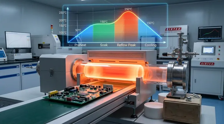
The Four Stages of the Reflow Profile
A reflow profile is a time-temperature graph that a printed circuit board (PCB) follows during the soldering process. Each stage serves a specific purpose, and getting any one of them wrong can lead to manufacturing defects.
Stage 1: The Preheat Zone
The initial stage involves raising the temperature of the entire board assembly at a controlled rate, typically 1-3°C per second.
This gradual ramp-up prevents thermal shock, which can crack components or the PCB itself. It also begins to activate the flux in the solder paste, which starts the cleaning process on the component leads and PCB pads.
Stage 2: The Thermal Soak Zone
Next, the assembly is held at a stable temperature, usually between 150°C and 200°C, for 60 to 120 seconds.
This stage allows the temperatures across the entire board to equalize. It ensures that large components heat up at the same rate as small ones, and it gives the flux sufficient time to activate fully and remove oxides before soldering.
Stage 3: The Reflow Zone
This is the critical phase where the oven temperature rises above the solder's melting point (its liquidus temperature).
For common lead-free solders (like Sn/Ag/Cu alloys), the peak temperature reaches 240°C to 250°C. The assembly stays in this zone just long enough—typically 30 to 90 seconds—for the solder paste to melt completely, flow (or "wet"), and form strong metallurgical bonds.
Stage 4: The Cooling Zone
Finally, the board is cooled at a controlled rate. The cooling rate is just as important as the heating rate.
Cooling too slowly can lead to brittle solder joints. Cooling too quickly can induce thermal shock. The goal is to solidify the solder into a fine grain structure that provides optimal strength and reliability.
The Critical Risks: What Goes Wrong
Deviating from the ideal reflow profile introduces significant risks that can lead to immediate or latent product failures. Understanding these trade-offs is fundamental to process control.
The Problem with Too Much Heat
Exceeding the recommended peak temperature or time can cause component damage, delamination of the PCB layers, and oxidation of the solder joint. It can also lead to a defect called "tombstoning," where a small component lifts off one pad and stands vertically.
The Danger of Too Little Heat
Insufficient heat or time during the reflow stage results in incomplete melting of the solder. This creates weak, unreliable connections known as "cold joints." It can also cause poor "wetting," where the solder fails to flow properly and bond with the component lead and pad.
Making the Right Choice for Your Board
The ideal reflow profile is not universal; it must be tailored to the specific components, solder paste, and board design you are using.
- If your board uses heat-sensitive components: Your primary focus must be on keeping the peak temperature as low and the time-above-liquidus as short as possible while still achieving a valid solder joint.
- If your board has large components mixed with small ones: The thermal soak stage is your most critical tool for ensuring all parts of the board reach a uniform temperature before the final reflow spike.
- If you are using a specific solder paste: Always start with the manufacturer's datasheet, which provides the recommended thermal profile for that exact chemical composition.
Ultimately, mastering the reflow process is about achieving a precise thermal balance across the entire assembly.
Summary Table:
| Stage | Temperature Range | Duration | Key Purpose |
|---|---|---|---|
| Preheat | Gradual Ramp (1-3°C/sec) | - | Prevent thermal shock, activate flux |
| Soak | 150°C - 200°C | 60-120 sec | Equalize board temperature, fully activate flux |
| Reflow | 240°C - 250°C (Peak) | 30-90 sec | Melt solder for strong metallurgical bonds |
| Cooling | Controlled Rate | - | Solidify solder for optimal joint strength |
Achieve Perfect Solder Joints with Precision Thermal Control
Struggling with tombstoning, cold joints, or component damage? KINTEK specializes in lab equipment and consumables for electronics manufacturing, including precision reflow ovens and thermal profiling solutions. Our expertise helps you:
- Optimize your reflow profile for specific components and solder pastes
- Prevent manufacturing defects with precise temperature control
- Enhance product reliability through consistent thermal management
Let our team help you master the reflow process. Contact KINTEK today for a personalized consultation on your soldering challenges!
Visual Guide
Related Products
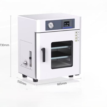
- 56L Vertical Laboratory Vacuum Drying Oven
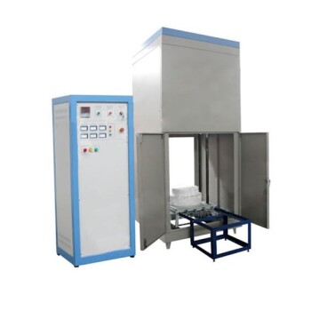
- High Temperature Muffle Oven Furnace for Laboratory Debinding and Pre Sintering
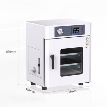
- 23L Laboratory Vacuum Drying Oven
- Laboratory Scientific Electric Heating Blast Drying Oven
- Graphite Vacuum Furnace High Thermal Conductivity Film Graphitization Furnace
People Also Ask
- Why is a vacuum drying oven recommended for the post-processing of recovered cadmium sponge? | KINTEK
- What role does a laboratory vacuum drying oven play in processing nanoparticle powder samples? Protect Sample Integrity
- Why is a laboratory vacuum drying oven recommended for rice straw residues? Protect Your Biomass Integrity
- Why is a Laboratory Vacuum Drying Oven recommended for PBAT microspheres? Protect Sensitive Polymer Integrity
- Why must a vacuum drying oven be used after preparing composite electrolytes? Ensure Battery Stability and Purity