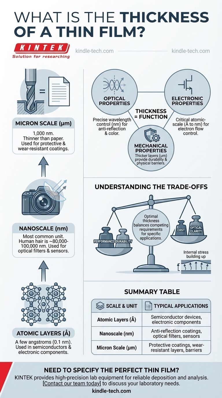
A thin film's thickness is not a single value but a precisely engineered dimension that can range from a single layer of atoms (a few angstroms or tenths of a nanometer) to several micrometers. This thickness is the most critical parameter that defines how the film will function, as it is meticulously controlled during manufacturing to achieve specific optical, electronic, or mechanical properties.
The essential insight is that a film's thickness is not an arbitrary measurement, but a direct consequence of its intended purpose. The correct question is not "how thick is a film?" but "what must the film do?". Thickness is the primary design parameter used to achieve that function.
Why "Thickness" Isn't One Number
The vast range in thin film thickness exists because the term "thin film" covers an enormous variety of applications. The required thickness is determined entirely by the physics of the problem it is designed to solve.
It's Defined by Function, Not a Rule
A film's purpose dictates its thickness. An anti-reflection coating on a camera lens is engineered to be a specific fraction of a light's wavelength, often just tens of nanometers thick.
In contrast, a layer in a semiconductor device might be just a few atoms thick to control electron flow, while a protective coating on a tool bit might be several micrometers thick for durability.
The Scale: From Atoms to Microns
To grasp the range, it helps to understand the units. Film thickness is most commonly measured in nanometers (nm).
- Angstrom (Å): The smallest unit used, equal to 0.1 nm. This scale is used for films that are only a few atomic layers thick.
- Nanometer (nm): The most common unit. A human hair is roughly 80,000-100,000 nm thick.
- Micrometer (µm): Also called a micron, it equals 1,000 nm. Films in the micron range are considered thick but are still far thinner than a sheet of paper.
The Influence of Deposition and Substrate
The final properties of a film depend not just on its thickness but also on the material it's placed upon (substrate) and the manufacturing method (deposition technique). These factors influence the film's density, uniformity, and internal stress, which all work together with thickness to produce the desired outcome.
How Thickness Determines a Film's Properties
Altering a film's thickness by even a few nanometers can completely change its behavior. This is because thickness directly interacts with physical phenomena like light waves and electrons.
Optical Properties: The Science of Interference
For optical coatings, thickness is paramount. Light reflecting from the top surface of the film interferes with light reflecting from the bottom surface.
By controlling the film's thickness to be, for example, one-quarter of a specific light wavelength, engineers can cause these reflected waves to cancel each other out, creating a highly effective anti-reflection coating. Change the thickness, and you change the color and wavelength of light it affects.
Electronic Properties: Building a Semiconductor
In microchips, thin films are the building blocks of transistors. Extremely thin insulating films (gate oxides) just a few nanometers thick are used to control the flow of electrons.
If this film is too thick, the device won't switch properly. If it's too thin, electrons can leak through, causing the chip to fail.
Mechanical and Chemical Properties: Creating a Barrier
For protective applications like scratch-resistant coatings on eyeglasses or corrosion-resistant layers on metal, thickness often correlates with durability. A thicker film can provide a more robust physical barrier against wear and environmental damage.
Understanding the Trade-offs
Choosing a film's thickness is always an act of balancing competing requirements. There is no single "best" thickness, only the optimal one for a specific application.
Performance vs. Cost
Achieving highly precise and uniform thickness, especially at the nanometer scale, requires sophisticated and expensive deposition equipment. A thicker, less precise film is often much cheaper to produce.
Durability vs. Optical Clarity
For a protective coating on a lens, making the film thicker might increase its scratch resistance. However, a thicker film can also absorb or scatter more light, potentially reducing the optical performance of the lens.
Function vs. Material Stress
As films are deposited, internal stresses can build up. A very thick film might be more durable but could have so much internal stress that it cracks or peels away from the substrate, rendering it useless.
Making the Right Choice for Your Goal
Your application's primary goal will be the definitive guide for determining the required film thickness.
- If your primary focus is optical performance: Your film thickness will be precisely calculated in nanometers to manipulate specific wavelengths of light, such as for filters or anti-reflection coatings.
- If your primary focus is electronic function: You will work with stacked layers where each film's thickness, often measured in angstroms or nanometers, is critical for creating functional device structures like transistors.
- If your primary focus is mechanical protection: Your film may be thicker, often in the higher nanometer to micron range, to provide a durable physical barrier against wear or corrosion.
Ultimately, a thin film's thickness is the physical expression of its intended purpose.
Summary Table:
| Thickness Scale | Common Unit | Typical Applications |
|---|---|---|
| Atomic Layers | Angstroms (Å) | Semiconductor devices, electronic components |
| Nanoscale | Nanometers (nm) | Anti-reflection coatings, optical filters, sensors |
| Micron Scale | Micrometers (µm) | Protective coatings, wear-resistant layers, barriers |
Need to Specify the Perfect Thin Film for Your Project?
Determining the optimal thickness is critical for achieving the desired optical, electronic, or mechanical performance in your application. KINTEK specializes in providing the high-precision lab equipment and consumables necessary for reliable thin film deposition and analysis.
Let our experts help you select the right tools to control this essential parameter. Contact our team today to discuss your specific laboratory needs and ensure your project's success.
Visual Guide
Related Products
- RF PECVD System Radio Frequency Plasma-Enhanced Chemical Vapor Deposition RF PECVD
- Chemical Vapor Deposition CVD Equipment System Chamber Slide PECVD Tube Furnace with Liquid Gasifier PECVD Machine
- Microwave Plasma Chemical Vapor Deposition MPCVD Machine System Reactor for Lab and Diamond Growth
- Cylindrical Resonator MPCVD Machine System Reactor for Microwave Plasma Chemical Vapor Deposition and Lab Diamond Growth
- Aluminized Ceramic Evaporation Boat for Thin Film Deposition
People Also Ask
- How does RF power create plasma? Achieve Stable, High-Density Plasma for Your Applications
- What is plasma activated chemical vapour deposition method? A Low-Temperature Solution for Advanced Coatings
- What are the advantages of PECVD? Enable Low-Temperature, High-Quality Thin-Film Deposition
- How are PECVD and CVD different? A Guide to Choosing the Right Thin-Film Deposition Process
- What are the benefits of PECVD? Achieve Superior Low-Temperature Thin Film Deposition