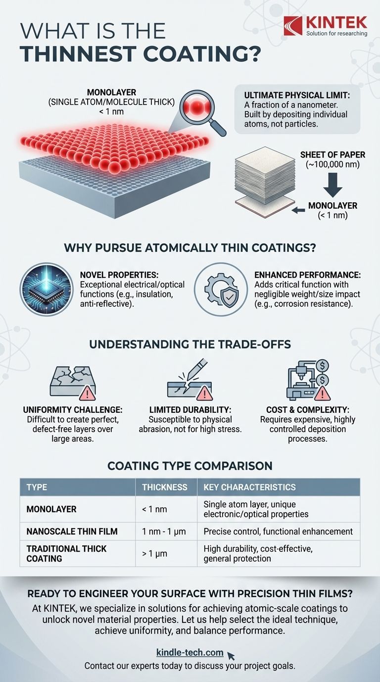
The thinnest possible coating is a monolayer, which is a single, unbroken layer of atoms or molecules. This represents the ultimate physical limit of thinness, often measuring just a fraction of a nanometer thick. These coatings fall into the category of "thin films," which are created by depositing individual atoms or molecules onto a substrate surface.
The pursuit of thinner coatings is not just about minimalism; it's about unlocking unique properties that only emerge at the atomic scale. The thinnest coating is a single atomic layer, shifting the goal from simple protection to precisely engineering the fundamental electrical, optical, and physical properties of a surface.
What Defines the "Thinnest" Coating?
The concept of the "thinnest coating" is defined by the physical limits of matter itself. Reaching this limit requires specialized processes that operate at an atomic level.
The Concept of a Monolayer
A true monolayer is the theoretical limit. It's a contiguous layer just one atom or one molecule thick.
Anything less than a complete monolayer would result in an incomplete coating with gaps, failing to cover the entire substrate.
Measuring in Nanometers
Thin films are measured in nanometers (nm), with the thinnest being a fraction of a nanometer.
To put this in perspective, a single sheet of paper is about 100,000 nanometers thick. An atomic-level coating is hundreds of thousands of times thinner.
Built from Atoms, Not Particles
The key difference between an ultra-thin film and a conventional thick coating is how it's applied.
Thick coatings, like paint, involve applying larger particles. True thin films are built by meticulously depositing individual atoms or molecules, which allows for this incredible level of precision and control.
Why Pursue Atomically Thin Coatings?
Applying a coating that is only a few atoms thick is done to achieve specific functional outcomes that thicker layers cannot provide. The goal is performance enhancement, not just coverage.
Unlocking Novel Properties
At this scale, a material's properties can change dramatically. A coating can be engineered to provide exceptional electrical insulation or conductivity, or to have specific optical transmission properties, such as being anti-reflective.
Enhancing Surface Performance
An atomically thin layer can add critical functionality with negligible impact on the component's weight or dimensions.
This is vital in fields like microelectronics and optics, where even tiny changes in size can affect performance. A thin film can add corrosion resistance or other protective benefits to a delicate substrate.
Understanding the Trade-offs
While monolayers represent a pinnacle of material science, they are not a universal solution. The practical challenges are significant and dictate where they can be effectively used.
The Challenge of Uniformity
Creating a perfect, defect-free monolayer over a large surface area is exceptionally difficult.
This process requires highly controlled environments, such as a vacuum, to prevent impurities from disrupting the atomic layer as it forms.
Durability and Wear
By its very nature, a single layer of atoms is not as mechanically robust as a thicker coating.
These films are susceptible to damage from physical abrasion and are best suited for applications where they are not exposed to significant mechanical stress.
Cost and Complexity
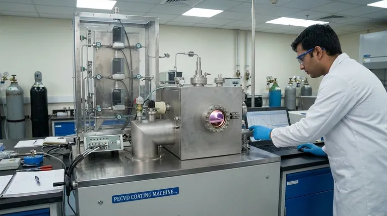
The deposition processes required to create atomic-level thin films are far more complex and expensive than traditional coating methods.
The investment in equipment and process control is substantial, limiting its use to high-value applications where the unique properties are absolutely necessary.
Making the Right Choice for Your Goal
Choosing the right coating thickness depends entirely on balancing performance requirements, durability, and cost.
- If your primary focus is ultimate thinness and unique electronic or optical properties: A monolayer or few-layer thin film is the target, but you must be prepared for complex and costly deposition processes.
- If your primary focus is general durability and corrosion resistance: A traditional thick coating or a multi-micron thin film is a far more practical and cost-effective solution.
- If your primary focus is adding a specific function without altering dimensions: Thin films in the nanometer range offer an excellent balance of performance and practicality for many advanced applications.
Ultimately, the concept of the "thinnest coating" pushes the boundaries of material science, transforming a simple protective layer into a functional, highly engineered surface.
Summary Table:
| Coating Type | Typical Thickness | Key Characteristics | Primary Applications |
|---|---|---|---|
| Monolayer | < 1 nm | Single layer of atoms/molecules, unique electronic/optical properties | Microelectronics, advanced optics, sensors |
| Nanoscale Thin Film | 1 nm - 1 μm | Precise thickness control, functional surface enhancement | Semiconductors, protective coatings, optical filters |
| Traditional Thick Coating | > 1 μm | High durability, cost-effective application | General corrosion protection, paints, structural coatings |
Ready to Engineer Your Surface with Precision Thin Films?
Whether you're developing cutting-edge microelectronics, advanced optical components, or specialized sensors, the right coating thickness is critical to your success. At KINTEK, we specialize in lab equipment and consumables for thin film deposition and surface engineering. Our solutions help researchers and manufacturers achieve the precise, atomic-scale coatings needed to unlock novel material properties.
Let us help you:
- Select the ideal deposition technique for your application
- Achieve uniform, defect-free thin films
- Balance performance requirements with practical considerations
Contact our experts today to discuss how our specialized equipment can advance your thin film projects!
Visual Guide
Related Products
- Electrolytic Electrochemical Cell for Coating Evaluation
- Infrared Transmission Coating Sapphire Sheet Substrate Window
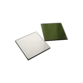
- 400-700nm Wavelength Anti Reflective AR Coating Glass
- Electron Beam Evaporation Coating Oxygen-Free Copper Crucible and Evaporation Boat
- Aluminum-Plastic Flexible Packaging Film for Lithium Battery Packaging
People Also Ask
- What is the procedure for starting the experiment and what should be observed? A Step-by-Step Guide for Reliable Electrochemistry
- What materials are the coating evaluation electrolytic cell and its lid made of? Ensuring Accurate Electrochemical Testing
- What is the difference between a voltaic cell and an electrochemical cell? Understand the Two Types of Energy Conversion
- What type of electrode system is the coating evaluation electrolytic cell designed for? Unlock Precise Coating Analysis
- What is the correct shutdown and disassembly procedure after an experiment? Ensure Safety and Protect Your Equipment