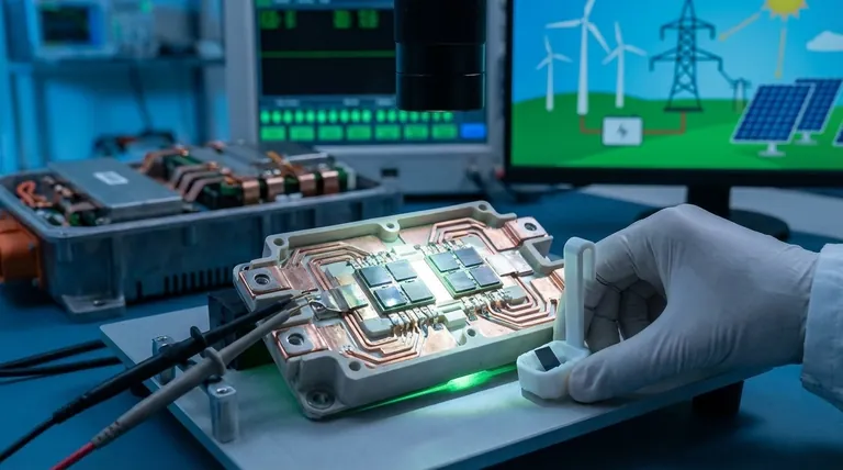
At its core, Silicon Carbide (SiC) is a semiconductor material used to build electronic components that are more efficient, smaller, and more robust than those made from traditional silicon. It excels in applications that involve high power, high voltage, high frequencies, and high temperatures, making it a critical enabler for technologies like electric vehicles and renewable energy systems.
Silicon Carbide is not a universal replacement for silicon. Instead, it is a specialized, high-performance material that solves the physical limitations of silicon in power electronics, allowing us to build systems that waste less energy, run cooler, and fit into smaller spaces.
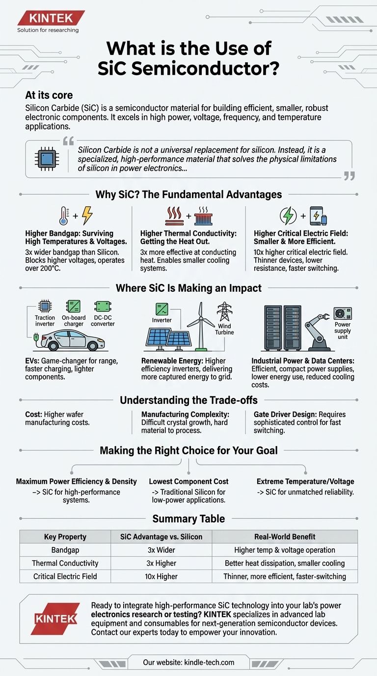
Why SiC? The Fundamental Advantages
The reason SiC is transforming power electronics lies in its superior material properties compared to silicon (Si). These properties directly translate into tangible performance gains in real-world devices.
Higher Bandgap: Surviving High Temperatures and Voltages
A semiconductor's bandgap is the energy required to excite an electron into a conductive state. SiC has a bandgap roughly three times wider than that of silicon.
This wide bandgap means SiC devices can block significantly higher voltages before breaking down and can operate reliably at much higher temperatures (over 200°C) where silicon components would fail.
Higher Thermal Conductivity: Getting the Heat Out
SiC is approximately three times more effective at conducting heat away from the device than silicon.
This superior thermal conductivity means the waste heat generated during operation is removed more efficiently. This allows for smaller heat sinks and more compact overall system designs, a critical factor in applications like electric vehicles where space and weight are at a premium.
Higher Critical Electric Field: Smaller and More Efficient Devices
The critical electric field is the maximum field strength a material can withstand before electricity punches through it. SiC's is about ten times higher than silicon's.
This allows engineers to design SiC components that are much thinner for the same voltage rating. A thinner device has lower internal resistance, which dramatically reduces energy lost as heat (conduction losses) and enables faster switching speeds with less wasted energy (switching losses).
Where SiC Is Making an Impact
These fundamental advantages enable SiC to solve key challenges in several high-growth industries.
Electric Vehicles (EVs)
SiC is a game-changer for EVs. It is used in the main traction inverter, which converts DC power from the battery to AC power for the motor. The higher efficiency of SiC inverters directly translates to less energy wasted and a longer driving range from the same battery.
It is also used in on-board chargers (OBCs) and DC-DC converters, enabling faster charging and smaller, lighter power components throughout the vehicle.
Renewable Energy and Grid Infrastructure
In solar and wind energy systems, inverters are needed to convert the DC power generated by panels or turbines into grid-compatible AC power.
SiC-based inverters are significantly more efficient than their silicon counterparts, meaning more of the captured renewable energy is successfully delivered to the grid. Their high power density also allows for smaller and more cost-effective inverter stations.
Industrial Power and Data Centers
Modern data centers and industrial factories consume enormous amounts of power. SiC is used to build highly efficient and compact power supplies for servers, robotics, and industrial motor drives.
This reduces electricity consumption, lowers cooling costs, and frees up valuable physical space.
Understanding the Trade-offs
While its benefits are clear, SiC is not the solution for every problem. Its adoption involves navigating specific challenges.
The Challenge of Cost
The most significant barrier to widespread SiC adoption is cost. Manufacturing high-purity SiC wafers is a more complex and energy-intensive process than producing silicon wafers, resulting in a higher price per component.
Manufacturing Complexity
Growing large, defect-free SiC crystals is notoriously difficult. This slow growth process and the hardness of the material (which complicates slicing and polishing) contribute to the higher wafer cost and limit production volumes compared to the massive scale of the silicon industry.
Gate Driver Design
SiC devices, particularly MOSFETs, switch extremely fast. While this is a key advantage for efficiency, it also means they require more sophisticated and carefully designed gate driver circuits to control them properly and prevent electrical noise issues.
Making the Right Choice for Your Goal
Selecting between SiC and traditional silicon depends entirely on the specific requirements of your application.
- If your primary focus is maximum power efficiency and density: SiC is the definitive choice for high-performance systems where minimizing energy loss and size is more critical than initial component cost.
- If your primary focus is the lowest component cost for low-power applications: Traditional silicon remains the unbeatable standard for consumer electronics and systems where power demands are not extreme.
- If you are designing for extreme temperature or high-voltage environments: SiC provides a fundamental reliability advantage that silicon simply cannot match due to its physical properties.
Ultimately, Silicon Carbide empowers engineers to push past the boundaries of traditional electronics and build the next generation of efficient, powerful systems.
Summary Table:
| Key Property | SiC Advantage vs. Silicon | Real-World Benefit |
|---|---|---|
| Bandgap | 3x Wider | Higher temperature & voltage operation |
| Thermal Conductivity | 3x Higher | Better heat dissipation, smaller cooling systems |
| Critical Electric Field | 10x Higher | Thinner, more efficient, faster-switching devices |
Ready to integrate high-performance SiC technology into your lab's power electronics research or testing? KINTEK specializes in providing the advanced lab equipment and consumables needed to develop and validate next-generation semiconductor devices. Our solutions support the precise thermal management and material analysis critical for SiC applications. Contact our experts today to discuss how we can empower your innovation in electric vehicles, renewable energy, and beyond.
Visual Guide
Related Products
- Silicon Carbide (SIC) Ceramic Sheet Wear-Resistant Engineering Advanced Fine Ceramics
- Silicon Carbide (SIC) Ceramic Plate for Engineering Advanced Fine Ceramics
- Silicon Carbide (SIC) Ceramic Sheet Flat Corrugated Heat Sink for Engineering Advanced Fine Ceramics
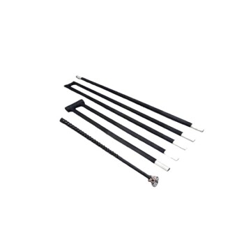
- Silicon Carbide SiC Thermal Heating Elements for Electric Furnace
- Infrared High Resistance Single Crystal Silicon Lens
People Also Ask
- What are the properties and applications of silicon carbide ceramics? Solve Extreme Engineering Challenges
- What are the uses of silicon carbide ceramics in different industries? Master Extreme Performance in Aerospace, Semiconductors & More
- What is the temperature resistance of silicon carbide? Withstands Extreme Heat Up to 1500°C
- What are the applications of silicon carbide? From Abrasives to High-Tech Semiconductors
- What are the properties of SiC? Unlock High-Temperature, High-Frequency Performance