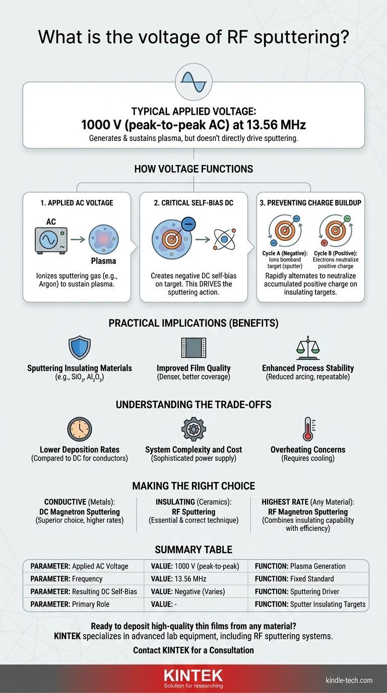
In RF sputtering, the typical applied voltage is a 1000 V peak-to-peak alternating current (AC) signal. This high-frequency signal, almost universally fixed at 13.56 MHz, is used to generate and sustain a plasma. However, the key to the process is the creation of an effective negative DC "self-bias" voltage on the target material, which is what actually drives the sputtering action.
The core concept is not the applied AC voltage itself, but the negative DC self-bias it creates. This unique mechanism allows RF sputtering to effectively deposit insulating materials by preventing the charge buildup that would otherwise halt the process in a standard DC system.
How Voltage Functions in RF Sputtering
To understand RF sputtering, it's crucial to distinguish between the AC signal that powers the system and the resulting DC voltage that does the work.
The Applied AC Voltage
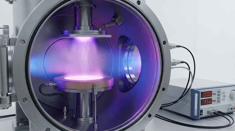
The RF power supply delivers a high-frequency AC signal, typically 1000 volts peak-to-peak at 13.56 MHz. The primary purpose of this signal is to ionize a sputtering gas (like Argon) by stripping electrons from the atoms, creating a sustained plasma within the vacuum chamber.
The Critical Self-Bias DC Voltage
Once the plasma is formed, the system cleverly uses the AC signal to create a constant negative DC voltage on the target. Because the target electrode is smaller than the chamber walls, the plasma effectively acts as a rectifier.
This process creates an average negative voltage, known as the self-bias, directly on the surface of the target material. It is this negative self-bias that attracts the positive gas ions from the plasma, accelerating them with enough force to bombard the target and eject, or "sputter," atoms.
Preventing Insulator Charge Buildup
This two-part voltage system is the fundamental reason RF sputtering works on insulating materials.
In a DC system, bombarding an insulator with positive ions would cause a positive charge to build up on its surface, eventually repelling any more incoming ions and stopping the sputtering process entirely.
In an RF system, the voltage rapidly alternates. During the negative cycle, ions bombard the target. During the brief positive cycle, the target attracts electrons from the plasma, which neutralize the accumulated positive charge from the previous cycle. This allows the process to continue indefinitely without interruption.
Practical Implications of the RF Method
The unique voltage mechanics of RF sputtering lead to several distinct advantages and applications compared to other deposition techniques.
Sputtering Insulating Materials
This is the primary advantage. RF sputtering is the industry-standard method for depositing dielectric materials like silicon dioxide (SiO₂), aluminum oxide (Al₂O₃), and other ceramics that cannot be deposited with DC sputtering.
Improved Film Quality
RF sputtering can sustain a plasma at much lower chamber pressures (typically 1-15 mTorr). At these low pressures, sputtered atoms travel from the target to the substrate with fewer gas collisions, resulting in a more direct path and leading to denser, higher-quality films with better coverage over surface features.
Enhanced Process Stability
The AC nature of the power source significantly reduces arcing, which is a common problem in DC systems. This, combined with newer developments like RF Diode sputtering that create more uniform target erosion, leads to a highly stable and repeatable deposition process.
Understanding the Trade-offs
While powerful, RF sputtering is not the ideal solution for every scenario. It involves clear trade-offs in performance and complexity.
Lower Deposition Rates
Compared to DC sputtering for conductive materials, RF sputtering is generally slower. The alternating cycle means that sputtering is not occurring 100% of the time, and the overall power transfer can be less efficient.
System Complexity and Cost
An RF sputtering system requires a sophisticated high-frequency power supply and an impedance matching network to efficiently transfer power to the plasma. This makes the equipment more complex and expensive than a standard DC power supply.
Overheating Concerns
Generating a stable RF plasma requires a significant power input. This can lead to overheating of the target material, which must be managed with an effective cooling system to ensure process stability and prevent damage to the target.
Making the Right Choice for Your Goal
The choice between sputtering techniques ultimately depends on the electrical properties of the material you need to deposit.
- If your primary focus is on conductive materials (metals): DC magnetron sputtering is generally the superior choice, offering higher deposition rates and lower equipment cost.
- If your primary focus is on insulating materials (ceramics, oxides): RF sputtering is the essential and correct technique, as it is specifically designed to overcome the issue of target charging.
- If your primary focus is achieving the highest possible deposition rate on any material: RF magnetron sputtering combines the insulating capabilities of RF with the plasma-confining efficiency of a magnetron to deliver the best of both worlds.
Ultimately, understanding how voltage enables RF sputtering allows you to select the precise tool needed to fabricate high-quality thin films from any class of material.
Summary Table:
| Key Voltage Parameter | Typical Value / Function |
|---|---|
| Applied AC Voltage | 1000 V (peak-to-peak) |
| Frequency | 13.56 MHz |
| Resulting DC Self-Bias | Negative voltage on target (varies) |
| Primary Role | Sputtering atoms from insulating targets |
Ready to deposit high-quality thin films from any material?
Whether your research involves conductive metals or complex insulating ceramics, choosing the right sputtering system is critical for success. KINTEK specializes in advanced lab equipment, including RF sputtering systems, to meet your precise deposition needs.
We provide the tools and expertise to help you achieve dense, uniform films with superior process stability. Contact us today to discuss how our solutions can enhance your laboratory's capabilities and accelerate your project timeline.
Contact KINTEK for a Consultation
Visual Guide
Related Products
- HFCVD Machine System Equipment for Drawing Die Nano-Diamond Coating
- 915MHz MPCVD Diamond Machine Microwave Plasma Chemical Vapor Deposition System Reactor
- Laboratory Sterilizer Lab Autoclave Vertical Pressure Steam Sterilizer for Liquid Crystal Display Automatic Type
- Laboratory Sterilizer Lab Autoclave Pulse Vacuum Lifting Sterilizer
- Vacuum Hot Press Furnace Machine for Lamination and Heating
People Also Ask
- How do CVD diamonds grow? A Step-by-Step Guide to Lab-Grown Diamond Creation
- What is the process of coating deposition? A Step-by-Step Guide to Thin Film Engineering
- What machine is used to make lab-grown diamonds? Discover the HPHT & CVD Technologies
- How is something diamond coated? A Guide to CVD Growth vs. Plating Methods
- What is microwave plasma CVD? A Guide to High-Purity Diamond and Material Synthesis