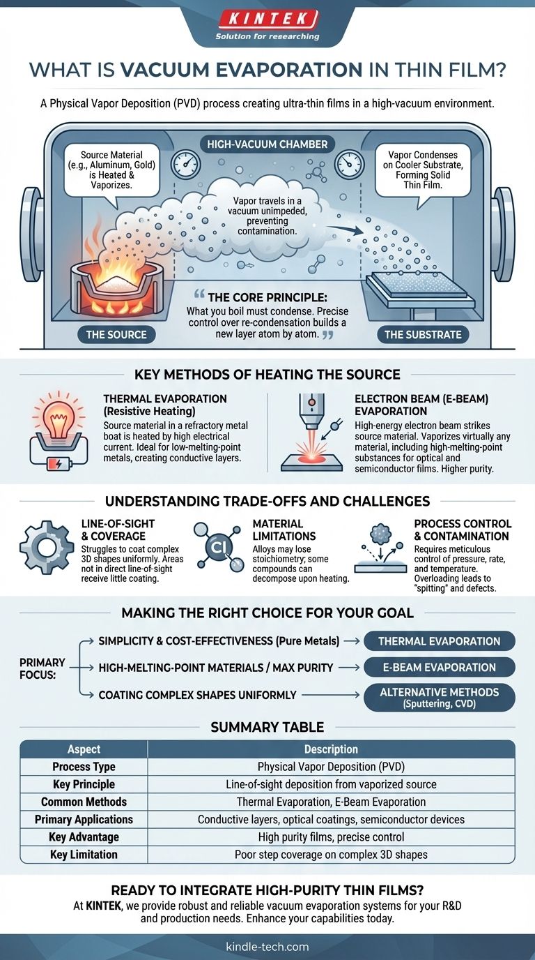
In essence, vacuum evaporation is a physical vapor deposition (PVD) process used to create extremely thin films of a material onto a surface, known as a substrate. The technique involves heating a source material inside a high-vacuum chamber until it vaporizes. These vaporized atoms or molecules then travel through the vacuum and condense onto the cooler substrate, forming a solid, uniform thin film.
The core principle behind vacuum evaporation is simple: what you boil must condense. By heating a material in a vacuum to turn it into a gas, you can precisely control its re-condensation onto a target surface, building a new layer one atom at a time.
The Core Principle: From Solid to Vapor to Film
Vacuum evaporation is a line-of-sight deposition method that relies on a straightforward physical transformation. Understanding the role of each component is key to understanding the process.
Why a Vacuum is Essential
A high-vacuum environment (low pressure) is critical for two reasons. First, it removes air and other gas molecules that could react with and contaminate the vaporized material.
Second, it allows the vaporized atoms to travel directly to the substrate without colliding with other particles. This unimpeded path is essential for creating a uniform and pure film.
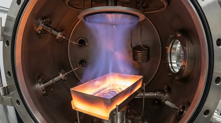
The Vaporization Step (The Source)
A source material, such as a pure metal like aluminum or gold, is placed inside the vacuum chamber. This source is then heated intensely until it begins to boil and evaporate, releasing a cloud of vapor.
The Deposition Step (The Substrate)
The vapor cloud expands and travels through the chamber, eventually reaching the substrate. Because the substrate is kept at a cooler temperature, the vapor condenses back into a solid upon contact, gradually building up the desired thin film.
Key Methods of Heating the Source
The primary difference between types of vacuum evaporation lies in how the source material is heated. The chosen method depends on the material being deposited and the required film quality.
Thermal Evaporation (Resistive Heating)
This is the most common and straightforward method. The source material is placed in a "boat" or coiled filament made of a refractory metal like tungsten. A high electrical current is passed through the boat, causing it to heat up rapidly and vaporize the material within it.
This method is ideal for depositing materials with lower melting points, such as pure metals, and is widely used for creating electrically conductive layers.
Electron Beam (E-Beam) Evaporation
For materials with very high melting points, like ceramics or refractory metals, thermal evaporation is insufficient. E-beam evaporation uses a high-energy beam of electrons, guided by magnetic fields, to strike and heat the source material directly.
The intense, focused energy can vaporize virtually any material. This allows for higher purity films and the deposition of a wider range of substances, including oxides and dielectrics for optical and semiconductor applications.
Understanding the Trade-offs and Challenges
While powerful, vacuum evaporation is not without its limitations. Success depends on navigating several key process variables and inherent constraints.
Line-of-Sight and Coverage
Because the vapor travels in a straight line from the source to the substrate, this method struggles to coat complex, three-dimensional shapes uniformly. Areas not in the direct "line of sight" of the source will receive little to no coating.
Material Limitations
Not all materials are suitable for evaporation. Alloys can be difficult to deposit with precise stoichiometry, as the constituent elements may have different evaporation rates. Some compounds can also decompose or react when heated, changing their chemical makeup during the process.
Process Control and Contamination
Achieving a perfectly uniform and pure film requires meticulous control over vacuum pressure, deposition rate, and temperature. Overloading the source material can lead to "spitting," where entire particles are ejected onto the substrate, creating defects.
Making the Right Choice for Your Goal
Selecting the correct deposition technique depends entirely on your material, budget, and desired film properties.
- If your primary focus is simplicity and cost-effectiveness for pure metals: Thermal evaporation is the most direct and economical path for applications like creating conductive contacts.
- If your primary focus is depositing high-melting-point materials or achieving maximum purity: E-beam evaporation provides the necessary energy and control for advanced optical and semiconductor films.
- If your primary focus is coating complex shapes uniformly: You should consider alternative methods like sputtering or Chemical Vapor Deposition (CVD), which do not rely on line-of-sight deposition.
Ultimately, vacuum evaporation is a foundational technique for building the microscopic structures that power our modern technology.
Summary Table:
| Aspect | Description |
|---|---|
| Process Type | Physical Vapor Deposition (PVD) |
| Key Principle | Line-of-sight deposition from vaporized source material |
| Common Methods | Thermal Evaporation, Electron Beam (E-Beam) Evaporation |
| Primary Applications | Conductive layers, optical coatings, semiconductor devices |
| Key Advantage | High purity films, precise control over deposition |
| Key Limitation | Poor step coverage on complex 3D shapes |
Ready to integrate high-purity thin films into your R&D or production?
At KINTEK, we specialize in providing robust and reliable lab equipment, including vacuum evaporation systems, to meet the precise demands of your laboratory. Whether you are working on semiconductor development, creating advanced optical coatings, or engineering new materials, our expertise ensures you have the right tools for superior results.
Contact our experts today to discuss your specific thin film deposition needs and discover how KINTEK can enhance your research and development capabilities.
Visual Guide
Related Products
- Molybdenum Tungsten Tantalum Evaporation Boat for High Temperature Applications
- Molybdenum Tungsten Tantalum Special Shape Evaporation Boat
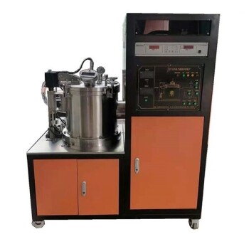
- Vacuum Induction Melting Spinning System Arc Melting Furnace
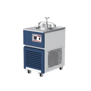
- Vacuum Cold Mounting Machine for Sample Preparation
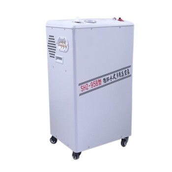
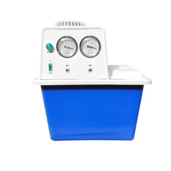
- Circulating Water Vacuum Pump for Laboratory and Industrial Use
People Also Ask
- What is the thermal evaporation method in thin film? A Guide to Simple, Cost-Effective PVD
- What are thermal evaporation sources? Key Types and How to Choose the Right One
- How does a molybdenum evaporation source function in H2S for MoS2 synthesis? Master Reactive Film Deposition
- What is the source of evaporation for thin film? Choosing Between Thermal and E-Beam Methods
- How source material is evaporated during deposition? A Guide to Resistive vs. E-Beam Methods