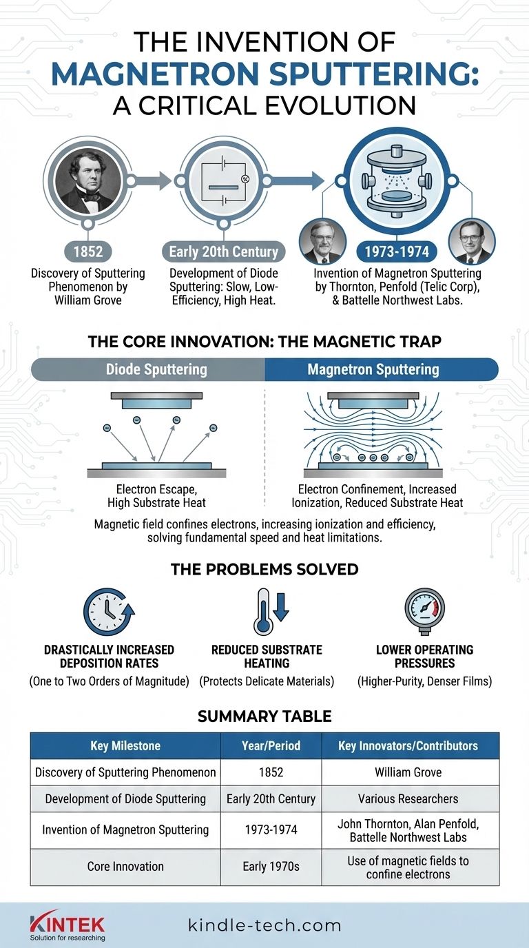
The foundational patents for modern magnetron sputtering were filed in the early 1970s. While the basic principle of sputtering was discovered much earlier, the development of a commercially viable, high-rate magnetron sputtering process is credited to researchers like John Thornton and Alan Penfold at Telic Corporation, as well as work done at Battelle Northwest Laboratories around 1973-1974.
The invention of magnetron sputtering was less a single discovery and more a critical evolution. By adding a magnetic field behind the sputtering target, engineers solved the fundamental limitations of speed and heat that had prevented sputtering from becoming a dominant industrial technology.
The Precursors: Understanding the Problem
Before magnetron sputtering, the primary method was diode sputtering. This earlier technique was useful in research but was too inefficient for many mass-production applications.
The Discovery of Sputtering
The underlying physical phenomenon was first observed by William Grove in 1852. He noted that a cathode in a discharge tube was gradually eroded, and the eroded material was deposited on nearby surfaces. This process, where ions bombard a target and eject atoms, is the basis of all sputtering.
The Limitations of Diode Sputtering
For over a century, diode sputtering remained a slow, low-efficiency process. Its primary drawbacks were low deposition rates and significant substrate heating.
The inefficiency stemmed from how electrons behaved. In a diode system, electrons escape the plasma and bombard the substrate, transferring a large amount of energy as heat. This limited the types of materials that could be coated and made the process far too slow for industrial use.
The Breakthrough: Confining Electrons
The genius of magnetron sputtering was the introduction of a permanent magnet array behind the target material. This seemingly simple addition completely changed the dynamics of the plasma.
The Core Innovation: The Magnetic Trap
The magnetic field creates a "tunnel" or trap for electrons directly in front of the target's surface. Instead of escaping and striking the substrate, the electrons are forced into a spiral path, greatly increasing their travel distance within the plasma.
This has two immediate and transformative effects. First, it dramatically increases the probability of an electron striking and ionizing a gas atom (typically Argon). Second, it confines the high-energy electrons away from the substrate.
The Result: A Stable, High-Density Plasma
With more ions being created, the bombardment of the target material becomes vastly more efficient. This creates a dense, stable plasma precisely where it's needed—right at the target surface.
This innovation directly solved the core problems of diode sputtering, turning a lab curiosity into an industrial powerhouse.
The Problems Magnetron Sputtering Solved
The invention wasn't just an incremental improvement; it was a fundamental shift that opened up new possibilities for manufacturing thin films.
Drastically Increased Deposition Rates
By creating a more intense and efficient ion bombardment, magnetron sputtering increased deposition rates by one to two orders of magnitude. Processes that once took hours could now be completed in minutes, making it viable for high-volume manufacturing of everything from microchips to architectural glass.
Reduced Substrate Heating
Because the magnetic field traps electrons near the target, the substrate is shielded from intense electron bombardment. This significantly lowers the heat load, allowing for the deposition of high-quality films onto heat-sensitive materials like plastics and polymers without causing damage.
Lower Operating Pressures
The improved ionization efficiency means a stable plasma can be maintained at much lower gas pressures. Sputtering at lower pressures results in fewer gas-phase collisions for the ejected target atoms, leading to higher-purity and denser thin films with better adhesion.
Understanding the Legacy of this Invention
The development of magnetron sputtering was a pivotal moment in materials science and manufacturing. Its benefits directly address the goals of most modern thin-film applications.
- If your primary focus is high-throughput manufacturing: The dramatic increase in deposition rates is the key legacy of this invention, enabling the cost-effective coating of large areas and complex parts.
- If your primary focus is coating delicate materials: The reduction in substrate heating, made possible by electron confinement, is the critical feature that allows for coating polymers, plastics, and other sensitive substrates.
- If your primary focus is high-quality optical or electronic films: The ability to operate at lower pressures results in purer, denser films with superior performance, a direct consequence of the magnetron's efficient plasma confinement.
Ultimately, the invention of magnetron sputtering transformed thin-film deposition from a specialized scientific process into a foundational industrial manufacturing technique.
Summary Table:
| Key Milestone | Year/Period | Key Innovators/Contributors |
|---|---|---|
| Discovery of Sputtering Phenomenon | 1852 | William Grove |
| Development of Diode Sputtering | Early 20th Century | Various Researchers |
| Invention of Magnetron Sputtering | 1973-1974 | John Thornton, Alan Penfold (Telic Corp), Battelle Northwest Labs |
| Core Innovation | Early 1970s | Use of magnetic fields to confine electrons |
Ready to leverage the power of modern magnetron sputtering in your lab? KINTEK specializes in high-performance lab equipment and consumables, providing solutions that deliver the high deposition rates, low substrate heating, and superior film quality essential for today's research and manufacturing. Our expertise helps laboratories achieve precise, efficient thin-film deposition. Contact us today to discuss how our sputtering systems can enhance your work!
Visual Guide
Related Products
- Microwave Plasma Chemical Vapor Deposition MPCVD Machine System Reactor for Lab and Diamond Growth
- Chemical Vapor Deposition CVD Equipment System Chamber Slide PECVD Tube Furnace with Liquid Gasifier PECVD Machine
- Molybdenum Tungsten Tantalum Special Shape Evaporation Boat
- Inclined Rotary Plasma Enhanced Chemical Vapor Deposition PECVD Equipment Tube Furnace Machine
- Inclined Rotary Plasma Enhanced Chemical Vapor Deposition PECVD Equipment Tube Furnace Machine
People Also Ask
- What pressure is needed for chemical vapor deposition of diamonds? Master the Low-Pressure 'Sweet Spot'
- How do vacuum pumps and valves collaborate in MPCVD? Achieve Precise Pressure Control for Superior CNT Synthesis
- How does a microwave plasma reactor facilitate the synthesis of diamond? Master MPCVD with Precision Technology
- How are CVD diamonds created? Discover the Science of Lab-Grown Diamond Precision
- How is a diamond formed from CVD? The Science of Growing Diamonds Atom by Atom