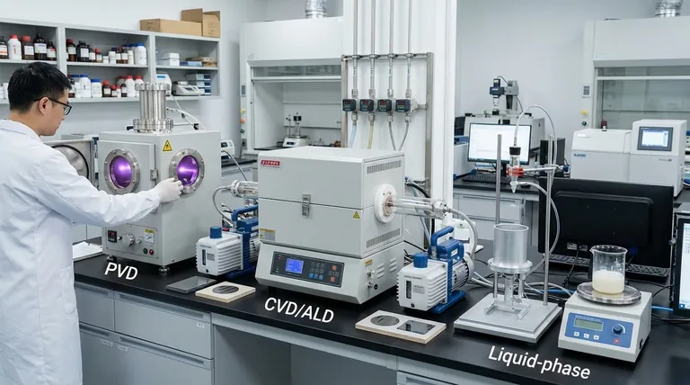
In short, thin film deposition methods are broadly classified into two primary categories: Physical Vapor Deposition (PVD) and Chemical Vapor Deposition (CVD). Specific techniques include sputtering and evaporation (for PVD), atomic layer deposition (for CVD), and other methods like sol-gel and spray pyrolysis that use liquid precursors.
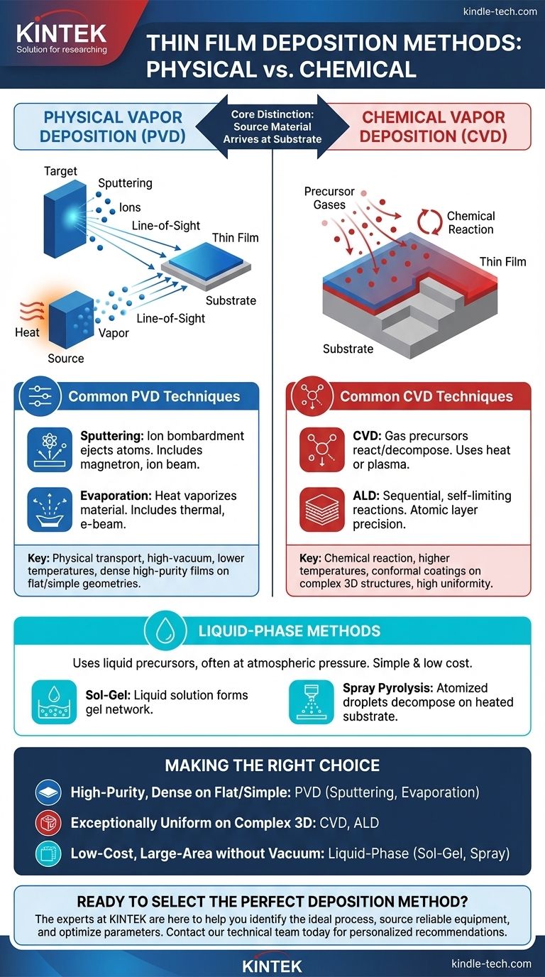
The core distinction lies in how the film material arrives at the substrate. Physical methods transport a vaporized solid material in a vacuum, while chemical methods use chemical reactions from gas or liquid precursors to form a solid film directly on the surface.
The Two Pillars of Deposition: Physical vs. Chemical
To truly understand thin film deposition, you must first grasp the fundamental difference between its two main philosophies: physical and chemical processes. Each approach has distinct mechanisms that determine the resulting film's properties and suitable applications.
Physical Vapor Deposition (PVD)
PVD is fundamentally a mechanical or thermal process. A solid source material, known as a "target," is vaporized in a high-vacuum environment, and the vaporized atoms travel to and condense on a substrate, forming the thin film.
Think of it as a highly controlled, atomic-scale spray-painting process. Because the atoms travel in a straight line, PVD is considered a line-of-sight technique.
Common PVD Techniques
Sputtering is a process where a target is bombarded with high-energy ions (typically from a gas like Argon), which physically ejects or "sputters" atoms from the target. These ejected atoms then deposit onto the substrate. Techniques include magnetron sputtering and ion beam sputtering.
Evaporation uses heat to turn the source material into a vapor. In thermal evaporation, the material is heated until it melts and evaporates, while electron beam (e-beam) evaporation uses a high-energy electron beam to vaporize the source material with great precision.
Chemical Vapor Deposition (CVD)
CVD is a chemical process where the substrate is exposed to one or more volatile precursor gases. These gases react or decompose on the substrate's surface to produce the desired solid film.
Unlike PVD, CVD is not a line-of-sight process. The precursor gases can flow around complex shapes, resulting in highly conformal coatings that uniformly cover intricate geometries.
Common CVD Techniques
The term CVD itself describes a broad family of processes that vary by pressure and the energy source used to drive the reaction (e.g., heat, plasma). It is a workhorse of the semiconductor industry.
Atomic Layer Deposition (ALD) is a highly advanced subclass of CVD. It uses a sequence of self-limiting chemical reactions to deposit material one atomic layer at a time, offering unparalleled precision in thickness and uniformity.
Exploring Liquid-Phase Methods
Beyond the dominant PVD and CVD vacuum techniques, a third category of chemical methods uses liquid precursors, often at or near atmospheric pressure. These are valued for their simplicity and low cost.
Sol-Gel Deposition
This method involves creating a "sol" (a solution of nanoscale particles) that is applied to a substrate, often by dipping or spinning. The substrate is then heated, causing the liquid to evaporate and the particles to form a solid, gel-like network that becomes the final film.
Spray Pyrolysis
In this technique, a liquid solution containing the desired film constituents is atomized into fine droplets and sprayed onto a heated substrate. The heat causes the droplets to evaporate and the precursors to decompose, forming a solid film on the surface.
Chemical Bath Deposition (CBD)
CBD involves simply immersing the substrate in a chemical solution. A controlled chemical reaction within the solution causes the desired material to slowly precipitate and deposit onto the substrate's surface.
Understanding the Trade-offs
No single deposition method is universally superior. The ideal choice is a direct function of the required film properties and the constraints of your application.
Conformal Coverage vs. Line-of-Sight
CVD and ALD excel at producing uniform, conformal films on complex, three-dimensional structures. The precursor gases can reach every exposed surface.
PVD methods are line-of-sight, making them perfect for coating flat surfaces but challenging for deep trenches or complex geometries, which can be "shadowed" from the source.
Deposition Temperature
Many CVD processes require high temperatures to drive the necessary chemical reactions. This can limit the types of substrates that can be used, particularly plastics or other temperature-sensitive materials.
PVD techniques, especially sputtering, can often be performed at much lower temperatures, offering greater flexibility with substrate materials.
Film Purity and Density
PVD methods like sputtering are known for producing very dense, high-purity films with strong adhesion. The physical bombardment process compacts the film as it grows.
CVD films are also very high-purity, but their density and microstructure can vary more depending on the specific chemistry and process conditions used.
Making the Right Choice for Your Application
Selecting the correct method requires aligning the process capabilities with your primary goal.
- If your primary focus is high-purity, dense coatings on flat or simple geometries: PVD methods like sputtering or e-beam evaporation are typically the most effective and direct choices.
- If your primary focus is exceptionally uniform coating on complex 3D structures: CVD, and particularly ALD for ultimate precision, are superior due to their non-line-of-sight, surface-reaction mechanism.
- If your primary focus is low-cost, large-area coating without high-vacuum requirements: Liquid-phase methods like sol-gel or spray pyrolysis offer a practical and scalable solution.
Ultimately, understanding the fundamental mechanism—physical transport versus chemical reaction—is the key to selecting the right tool for your specific engineering challenge.
Summary Table:
| Method Category | Key Techniques | Primary Mechanism | Best For |
|---|---|---|---|
| Physical Vapor Deposition (PVD) | Sputtering, Evaporation | Physical transport of vaporized solid | High-purity, dense films on flat/simple geometries |
| Chemical Vapor Deposition (CVD) | CVD, Atomic Layer Deposition (ALD) | Chemical reaction from gas precursors | Conformal coatings on complex 3D structures |
| Liquid-Phase Methods | Sol-Gel, Spray Pyrolysis | Chemical reaction from liquid precursors | Low-cost, large-area coating without high vacuum |
Ready to Select the Perfect Deposition Method for Your Project?
Choosing the right thin film deposition technique is critical to achieving your desired material properties and performance. The experts at KINTEK are here to help. We specialize in providing advanced lab equipment and consumables for all your deposition needs, whether you require the precision of PVD, the conformality of CVD/ALD, or the simplicity of liquid-phase methods.
We can help you:
- Identify the ideal process for your specific application and substrate.
- Source reliable equipment from leading manufacturers.
- Optimize your deposition parameters for superior results.
Let's discuss your project requirements. Contact our technical team today to get personalized recommendations and ensure your research or production is a success.
Visual Guide
Related Products
- Aluminized Ceramic Evaporation Boat for Thin Film Deposition
- Tungsten Evaporation Boat for Thin Film Deposition
- Electron Beam Evaporation Coating Oxygen-Free Copper Crucible and Evaporation Boat
- Molybdenum Tungsten Tantalum Evaporation Boat for High Temperature Applications
- Vacuum Hot Press Furnace Machine for Lamination and Heating
People Also Ask
- What are the applications of thin films deposition? Unlock New Possibilities for Your Materials
- Why are high-purity ceramic boats used for lignin activation? Ensure Purity & Thermal Stability
- What is thin film deposition? Unlock Advanced Surface Engineering for Your Materials
- What is the chemical method for thin film deposition? Build Films from the Molecular Level Up
- Why is an alumina boat and Ti3AlC2 powder bed necessary for Ti2AlC sintering? Protect MAX Phase Purity


