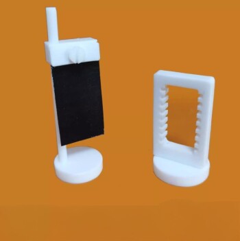
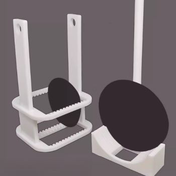
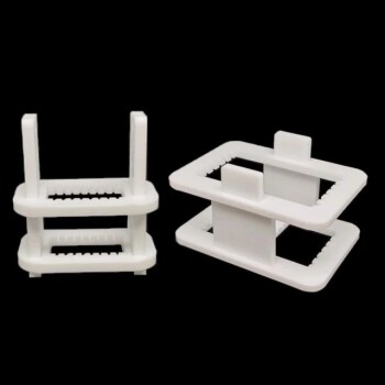
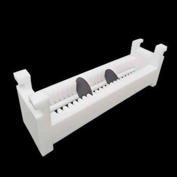
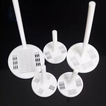
PTFE wafer fixtures are selected primarily for their exceptional chemical stability and extremely low surface friction. These fixtures are critical for handling silicon wafers after diamond nucleation because they minimize mechanical damage to the fragile nucleation layer and prevent the introduction of metallic or chemical impurities during transfer operations.
The choice of PTFE is driven by the need to preserve the integrity of the diamond nucleation layer; its low friction coefficient prevents physical scratching, while its chemical inertness ensures the wafer remains free of external contaminants.
Preserving Physical Integrity
The Importance of Low Friction
The diamond nucleation layer on a silicon wafer is incredibly fragile. PTFE (Polytetrafluoroethylene) possesses an extremely low surface friction coefficient.
This property ensures that when the wafer is slid into or out of the fixture, the material glides rather than abrades. This significantly reduces the risk of scratching or stripping the delicate nucleation sites.
Minimizing Mechanical Damage
Standard metal fixtures can create stress points or micro-abrasions on the wafer surface.
PTFE acts as a gentler interface during the operation and transfer of silicon wafers. Its inherent material properties cushion the wafer, protecting the structural uniformity of the nucleation layer.
Maintaining Chemical Purity
Superior Chemical Stability
PTFE is renowned for its chemical inertness and resistance to solvents, acids, and bases.
In the context of wafer processing, this stability ensures that the fixture itself does not react with the wafer or the surrounding process environment. It maintains its structural integrity without degrading over time.
Preventing Contamination
A critical requirement in semiconductor handling is the elimination of impurities.
Using PTFE fixtures prevents the introduction of metallic or chemical impurities that are common with other fixture materials. By eliminating leaching or particle shedding, PTFE protects the purity of the nucleation on the wafer surface.
Understanding the Trade-offs
Mechanical Rigidity vs. Protection
While PTFE is excellent for surface protection, it is a softer engineering plastic compared to metals like stainless steel or aluminum.
For applications requiring extreme structural rigidity or high-load bearing under pressure, PTFE fixtures may deform more easily than metallic alternatives. It is chosen when surface preservation outweighs the need for high tensile strength.
Thermal Considerations
PTFE handles high temperatures well, but it has a different coefficient of thermal expansion compared to silicon.
In environments with rapid, extreme temperature cycling, engineers must ensure the design accounts for expansion to prevent gripping the wafer too tightly or becoming too loose.
Making the Right Choice for Your Goal
To ensure the success of your diamond nucleation process, consider your specific handling requirements:
- If your primary focus is minimizing surface defects: Prioritize PTFE fixtures to utilize their low friction coefficient and prevent mechanical abrasion of the nucleation layer.
- If your primary focus is contamination control: Rely on PTFE to eliminate the risk of metallic ion transfer or chemical leaching that could compromise semiconductor performance.
By leveraging the unique properties of PTFE, you ensure that the critical nucleation layer remains physically intact and chemically pure throughout the handling process.
Summary Table:
| Feature | PTFE Advantage | Benefit for Diamond Nucleation |
|---|---|---|
| Surface Friction | Extremely Low | Prevents scratching and stripping of fragile nucleation sites |
| Chemical Stability | High Inertness | Ensures zero contamination from acids, bases, or solvents |
| Material Purity | Non-Metallic | Eliminates the risk of metallic ion transfer to silicon wafers |
| Physical Impact | Soft Interface | Cushions the wafer to minimize mechanical stress and micro-abrasions |
Maximize Your Semiconductor Yield with KINTEK Precision Solutions
Preserving the integrity of your diamond nucleation layer requires the highest standard of material purity and gentle handling. KINTEK specializes in high-performance laboratory equipment and consumables, offering a premium range of PTFE products, ceramics, and crucibles designed specifically for sensitive semiconductor processes.
Whether you are refining battery research or managing high-temperature furnace operations, our team provides the expertise and high-quality tools—from crushing and milling systems to high-pressure reactors—that your lab needs to succeed.
Don't compromise on purity. Contact KINTEK today to discover how our custom PTFE fixtures and laboratory consumables can optimize your wafer handling process.
References
- Oleg Babčenko, Alexander Kromka. GROWTH AND PROPERTIES OF DIAMOND FILMS PREPARED ON 4-INCH SUBSTRATES BY CAVITY PLASMA SYSTEMs. DOI: 10.37904/nanocon.2020.3701
This article is also based on technical information from Kintek Solution Knowledge Base .
Related Products
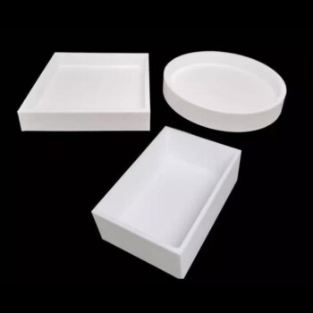
- Custom PTFE Teflon Parts Manufacturer for Hydrothermal Synthesis Reactor Polytetrafluoroethylene Carbon Paper and Carbon Cloth Nano-growth
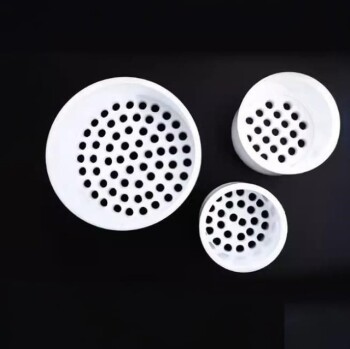
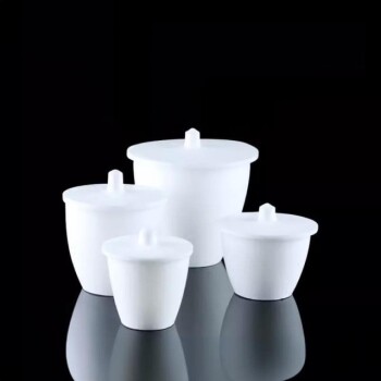
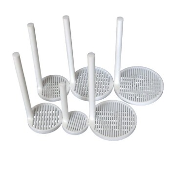
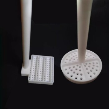
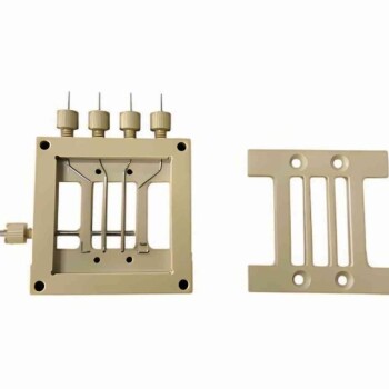
- Custom PTFE Wafer Holders for Lab and Semiconductor Processing
- Customizable PTFE Wafer Carriers for Semiconductor and Lab Applications
- Custom PTFE Teflon Parts Manufacturer for Conductive Glass Substrate Cleaning Rack
- Versatile PTFE Solutions for Semiconductor and Medical Wafer Processing
People Also Ask
- What is the purpose of using a PTFE-lined hydrothermal synthesis reactor? Prepare Superior LSGM Ceramic Precursors
- Why is a PTFE liner essential for the hydrothermal growth of copper sulfate nanocrystals? Protect Purity and Equipment
- Why is a PTFE Liner Essential for Hydrothermal Reactors? Protect Your Purity and Equipment
- What are the advantages of using polytetrafluoroethylene (PTFE) liners in hydrothermal synthesis reactors? High Purity
- What is the function of a PTFE-lined hydrothermal synthesis reactor in Silicalite-1 growth? Ensure High-Purity Crystals