Basic Principles and Applications of Graphite Crucibles
High-Temperature Melting and Heat Transfer
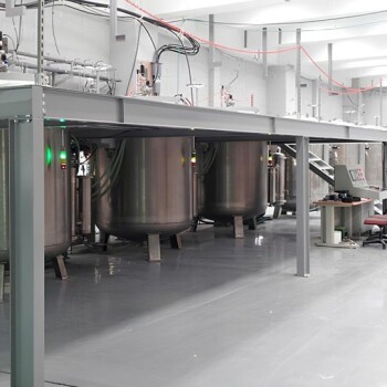
Graphite crucibles play a pivotal role in achieving the extreme temperatures necessary for the synthesis of third-generation semiconductor materials such as silicon carbide (SiC) and gallium nitride (GaN). These crucibles are designed to handle temperatures that can exceed 2000°C, making them indispensable in high-temperature processes like chemical vapor deposition (CVD) and physical vapor transport (PVT). The ability to maintain such high temperatures is critical for the uniform growth of semiconductor crystals, which directly impacts the quality and performance of the final product.
In addition to their thermal capabilities, graphite crucibles excel in providing uniform heat distribution. This uniformity is essential for the controlled growth of semiconductor crystals, ensuring that the material properties are consistent throughout the crystal structure. Non-uniform heat distribution can lead to defects and impurities, significantly reducing the efficiency and reliability of the semiconductor devices.
Moreover, the thermal conductivity of graphite crucibles is superior to many other materials, allowing for rapid heat transfer and efficient thermal management. This characteristic not only enhances the overall efficiency of the production process but also helps in maintaining the integrity of the crucible itself, thereby extending its service life. The combination of high-temperature resistance and excellent heat distribution makes graphite crucibles an indispensable tool in the production of advanced semiconductor materials.
Crystal Growth and Material Purification
Graphite crucibles play a pivotal role in the crystal growth and material purification processes, particularly in techniques such as Chemical Vapor Deposition (CVD) and Physical Vapor Transport (PVT). These crucibles are meticulously designed to maintain a highly controlled and pristine environment, which is essential for the production of high-quality semiconductor materials.
One of the primary functions of graphite crucibles in these processes is to prevent any unwanted chemical reactions and external contaminants from affecting the purity of the materials. This is achieved through the crucible's ability to create a barrier against environmental impurities, ensuring that the semiconductor compounds remain uncontaminated throughout the growth process.
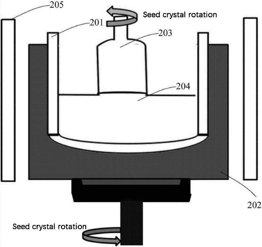
Moreover, the controlled growth environment facilitated by graphite crucibles is crucial for the uniform deposition of materials. This uniformity is key to achieving the desired crystal structure and properties, which are vital for the performance and reliability of the final semiconductor products. By maintaining a stable and controlled environment, graphite crucibles contribute significantly to the overall quality and efficiency of the semiconductor manufacturing process.
Technological Challenges and Solutions
High-Temperature Resistance and Oxidation
One of the primary challenges in the use of graphite crucibles for high-temperature applications, particularly in the production of third-generation semiconductor compounds, is the issue of thermal decay and oxidation. These challenges can significantly impact the performance and longevity of the crucibles, thereby affecting the overall efficiency and quality of the semiconductor materials produced.
To address these issues, several strategies have been developed. The first line of defense is the use of high-purity graphite. High-purity graphite is chosen for its superior thermal stability and resistance to degradation under extreme temperatures. This material is less prone to thermal decay, ensuring that the crucible maintains its structural integrity over extended periods of use.
In addition to high-purity graphite, antioxidant coatings play a crucial role in mitigating oxidation. Two of the most commonly used coatings are silicon carbide and boron nitride. These coatings act as protective barriers, preventing oxygen from penetrating the graphite and causing oxidative damage. Silicon carbide, known for its excellent thermal shock resistance and high melting point, is particularly effective in environments where high temperatures and rapid temperature changes are common. Boron nitride, on the other hand, offers exceptional chemical inertness and thermal conductivity, making it an ideal choice for protecting the crucible from both chemical and thermal degradation.
The combination of high-purity graphite and antioxidant coatings like silicon carbide or boron nitride provides a robust solution to the challenges of high-temperature resistance and oxidation. This dual approach not only enhances the durability and service life of the graphite crucibles but also ensures the consistent production of high-quality semiconductor materials.
Chemical Stability and Mechanical Strength
Ensuring the chemical stability of graphite crucibles and preventing thermal shock damage are paramount in the production of third-generation semiconductor compounds. This is achieved through meticulous material selection, the application of advanced coatings, and the optimization of crucible design.
Material selection plays a crucial role in maintaining chemical stability. High-purity graphite, for instance, is preferred due to its resistance to chemical reactions and its ability to withstand high temperatures without degrading. Additionally, coatings such as silicon carbide (SiC) or boron nitride (BN) are applied to enhance the crucible's resistance to oxidation and to provide a protective barrier against chemical attack.
The design of the crucible is equally important. Optimized designs not only enhance mechanical strength but also distribute thermal stress more evenly, thereby reducing the risk of thermal shock damage. This is particularly critical in processes that involve rapid temperature changes, such as those used in the growth of silicon carbide and gallium nitride crystals.
| Aspect | Importance | Solution |
|---|---|---|
| Chemical Stability | Prevents unwanted chemical reactions and contamination | Use of high-purity graphite and antioxidant coatings like SiC or BN |
| Thermal Shock Damage | Reduces risk of crucible failure during rapid temperature changes | Optimized design for even thermal stress distribution |
| Material Selection | Ensures resistance to high temperatures and chemical reactions | High-purity graphite for durability and stability |
| Coatings | Provides additional protection against oxidation and chemical interactions | Application of SiC or BN coatings for enhanced resistance |
By addressing these factors, manufacturers can ensure that graphite crucibles maintain their integrity and function effectively in the demanding environments of third-generation semiconductor production.
Service Life and Cost Control
Extending the service life of graphite crucibles and controlling costs are pivotal for the sustainable production of third-generation semiconductor compounds. This is achieved through a multifaceted approach that includes regular maintenance, the use of durable materials, and process optimization.
Regular Maintenance
Regular maintenance is crucial to ensure the longevity of graphite crucibles. This involves periodic inspections to identify and rectify any wear and tear, as well as to clean the crucibles to prevent contamination. For instance, thermal imaging can be used to monitor temperature distribution and detect any anomalies that could lead to premature failure. Additionally, ultrasonic testing can help identify internal cracks that are not visible to the naked eye, ensuring that only crucibles in optimal condition are used in production.
Durable Materials
The choice of materials significantly impacts the crucible's lifespan and cost-effectiveness. High-purity graphite, for example, offers superior resistance to high temperatures and chemical reactions, reducing the frequency of replacements and maintenance. Antioxidant coatings such as silicon carbide or boron nitride further enhance the crucible's durability by protecting against oxidation, a common cause of degradation in high-temperature environments.
Process Optimization
Optimizing the production process is another key strategy for extending crucible life and reducing costs. This includes fine-tuning parameters such as temperature control, heating and cooling rates, and the flow of reactive gases. For example, computer-aided design (CAD) and simulation software can be used to model and optimize these parameters, ensuring that the crucibles are operated under the most efficient conditions. Additionally, automated control systems can help maintain consistent process conditions, reducing the risk of human error and extending the crucible's operational life.
By integrating these strategies, manufacturers can significantly enhance the service life of graphite crucibles, thereby reducing overall production costs and supporting the sustainable growth of the semiconductor industry.
Future Trends in Graphite Crucible Development
Material Innovation and Manufacturing Process Optimization
Advancements in high-performance graphite materials and precision manufacturing technologies are set to revolutionize the performance of graphite crucibles, enabling them to meet increasingly stringent process requirements. These innovations are not merely incremental but represent a paradigm shift in the capability and reliability of crucibles used in the production of third-generation semiconductor compounds.
One of the key areas of innovation lies in the development of ultra-high purity graphite, which offers superior resistance to thermal decay and oxidation. This is particularly crucial for processes that demand extreme temperature stability, such as the Chemical Vapor Deposition (CVD) and Physical Vapor Transport (PVT) methods used in crystal growth. The integration of advanced antioxidant coatings, like silicon carbide or boron nitride, further enhances the crucible's durability and longevity, addressing one of the major challenges in high-temperature applications.
Precision manufacturing technologies are also playing a pivotal role in optimizing the design and fabrication of graphite crucibles. Techniques such as 3D printing and advanced machining processes allow for the creation of crucibles with intricate geometries and uniform thickness, which are essential for maintaining consistent heat distribution and preventing thermal shock damage. This level of precision ensures that the crucibles can withstand the rigors of continuous high-temperature operations without compromising on performance or lifespan.
Moreover, the adoption of automated quality control systems in the manufacturing process ensures that each crucible meets the highest standards of quality and reliability. These systems leverage machine learning algorithms to detect and rectify potential defects early in the production cycle, thereby minimizing waste and improving overall efficiency.
In summary, the convergence of material science breakthroughs and cutting-edge manufacturing technologies is poised to elevate the graphite crucible's role in semiconductor production, making it an indispensable component in the quest for high-quality, high-performance third-generation semiconductor materials.
Intelligence and Automation
The future of graphite crucible development is poised to benefit significantly from the integration of intelligent monitoring and automated control systems. These technologies are set to revolutionize the production processes of third-generation semiconductor compounds, enhancing both safety and efficiency.
Intelligent monitoring systems can provide real-time data analysis, allowing for immediate adjustments to process parameters. This capability is particularly crucial in high-temperature environments where even minor deviations can lead to significant material defects. By continuously tracking variables such as temperature, pressure, and chemical composition, these systems ensure that the conditions remain optimal for crystal growth and material purification.
Automation, on the other hand, can streamline operations by reducing human intervention. Automated control systems can execute complex sequences and respond to dynamic changes without manual oversight, thereby minimizing the risk of human error. This not only improves process consistency but also extends the service life of the graphite crucibles by preventing unnecessary wear and tear.
Moreover, the combination of intelligence and automation can lead to predictive maintenance, where systems anticipate potential issues before they escalate. This proactive approach can further enhance process safety and efficiency, ensuring that production runs smoothly and consistently.
In summary, the adoption of intelligent monitoring and automated control systems represents a pivotal advancement in the field of graphite crucible technology. By leveraging these technologies, the industry can achieve unprecedented levels of precision, safety, and efficiency in the production of third-generation semiconductor compounds.
Application Field Expansion and Cost-Effectiveness
The expansion of graphite crucibles into new materials and energy technologies, coupled with rigorous cost optimization strategies, is poised to significantly broaden their industrial applications. This expansion is not merely a lateral move but a strategic advancement that leverages the unique properties of graphite, such as its high-temperature resistance and chemical stability, to explore uncharted territories in material science and energy production.
For instance, the integration of graphite crucibles in emerging fields like advanced ceramics and renewable energy technologies, such as hydrogen production through high-temperature electrolysis, showcases their versatility and potential. These applications demand crucibles that can withstand extreme conditions while maintaining their structural integrity and performance, which graphite crucibles are uniquely suited to provide.
Moreover, the focus on cost optimization ensures that these advanced applications remain economically viable. By employing durable materials and optimizing manufacturing processes, the lifecycle costs of graphite crucibles can be significantly reduced, making them more accessible and attractive to industries seeking both high performance and cost efficiency. This dual approach of technological innovation and economic prudence not only enhances the marketability of graphite crucibles but also solidifies their role as indispensable tools in the evolving landscape of industrial and energy technologies.
Environmental Sustainability
In the quest for sustainable development, the production of third-generation semiconductor compounds must prioritize environmental sustainability. This involves a strategic shift towards the use of recyclable materials and the adoption of green technologies. By integrating these practices, the industry can significantly mitigate its environmental footprint.
Recyclable materials, such as high-purity graphite, play a pivotal role in reducing waste and conserving resources. These materials can be reused multiple times, thereby minimizing the need for raw material extraction and reducing the associated environmental costs. Additionally, the implementation of green technologies, such as energy-efficient manufacturing processes and the use of renewable energy sources, further enhances the sustainability of the production chain.
Moreover, the focus on environmental sustainability extends to the entire lifecycle of the graphite crucibles used in semiconductor production. From their manufacturing to their eventual disposal or recycling, these crucibles are designed to have minimal environmental impact. This holistic approach ensures that the industry not only meets current production demands but also contributes to a greener future.
Related Products
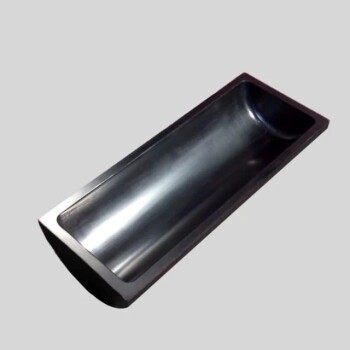
- High Purity Pure Graphite Crucible for Evaporation
- High Purity Pure Graphite Crucible for Electron Beam Evaporation
- Carbon Graphite Boat -Laboratory Tube Furnace with Cover
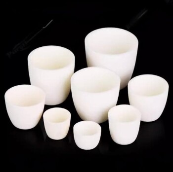
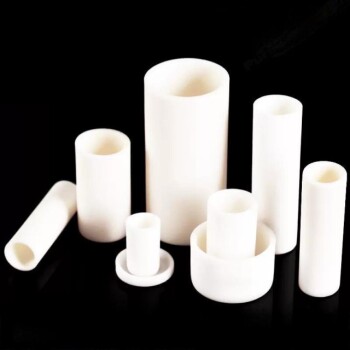
- Arc-Shaped Alumina Ceramic Crucible High Temperature Resistant for Engineering Advanced Fine Ceramics
- Engineering Advanced Fine Ceramics Alumina Al2O3 Crucible With Lid Cylindrical Laboratory Crucible