Introduction to Thin Film Deposition
Purpose and Process
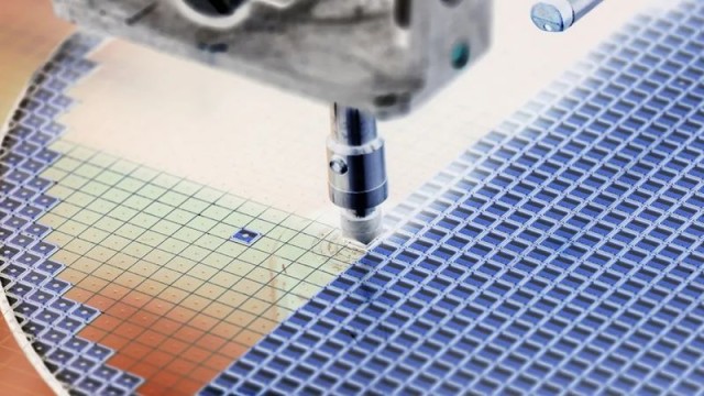
Thin film deposition is a critical process in semiconductor manufacturing, aimed at depositing a nano-scale thin film onto a substrate. This initial step is followed by a series of meticulous processes, including repeated etching and polishing, to create multiple stacked layers. These layers can be either conductive or insulating, each meticulously patterned to form intricate circuit designs.
The process of thin film deposition is integral to the integration of semiconductor components and circuits into complex chips. Each layer, once deposited and patterned, serves a specific function within the overall chip architecture, contributing to the chip's performance, reliability, and functionality. The precision and control inherent in thin film deposition processes are essential for ensuring that these layers adhere to the exacting standards required in modern semiconductor devices.
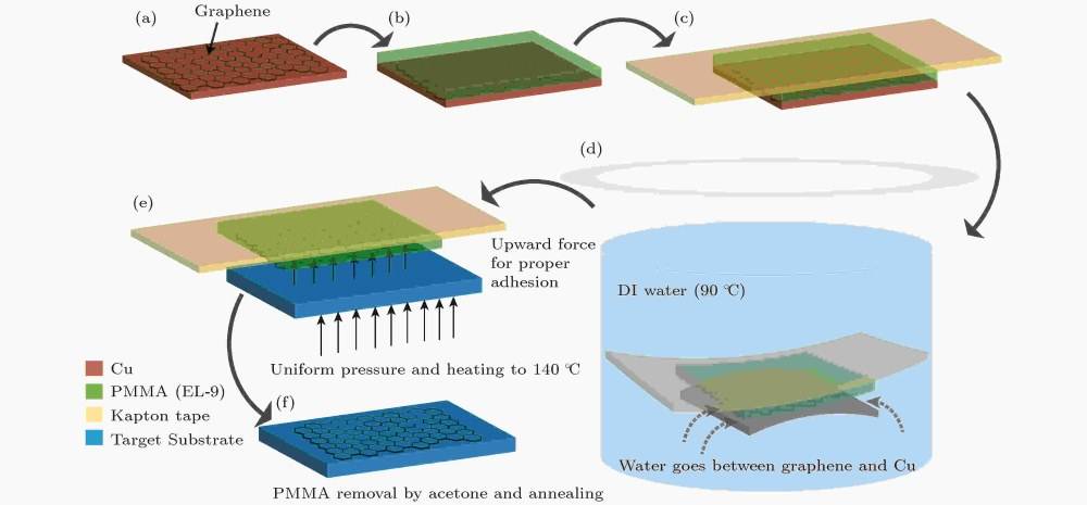
In essence, thin film deposition is not merely about creating layers; it is about building the foundational elements of semiconductor technology, layer by layer, to achieve the sophisticated and high-performance chips that power today's electronic devices.
Chemical Vapor Deposition (CVD)
Overview and Characteristics
Chemical Vapor Deposition (CVD) is a sophisticated technique that forms thin films through the thermal decomposition and/or reaction of gas compounds. This method offers a wide array of advantages, making it a cornerstone in semiconductor manufacturing. One of its primary strengths is its versatility in deposit types, allowing for the creation of a diverse range of materials with specific properties. This versatility is complemented by the ability to achieve uniform coatings across substrates, ensuring consistent performance and reliability in the final product.
High purity is another critical characteristic of CVD-deposited films. The controlled environment within the CVD reactor minimizes contamination, leading to films with minimal impurities. This high purity is essential for the performance and longevity of semiconductor devices, where even trace amounts of contaminants can significantly impact functionality.
Moreover, CVD provides precise control over the composition of the deposited films. By carefully selecting and regulating the gas compounds and reaction conditions, manufacturers can tailor the film's properties to meet specific requirements. This level of control is invaluable in the production of advanced semiconductor devices, where precise material properties are crucial for optimal performance.
However, one notable limitation of CVD is the requirement for high temperatures during the deposition process. These elevated temperatures can impose constraints on the types of substrates that can be used and may necessitate additional cooling and thermal management solutions. Despite this challenge, the benefits of CVD in terms of versatility, uniformity, purity, and composition control make it an indispensable technique in the semiconductor industry.
Stages of CVD Process
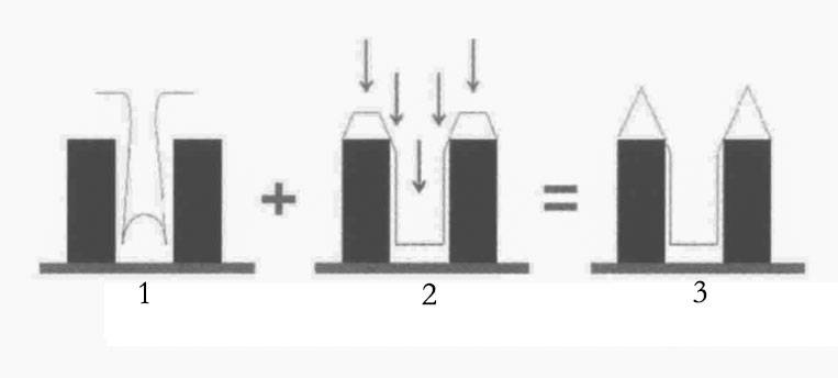
The Chemical Vapor Deposition (CVD) process is a multi-stage procedure that transforms gaseous precursors into a solid film on a substrate. This process is crucial for creating thin films with precise control over composition and thickness, which are essential for semiconductor manufacturing.
-
Gas Diffusion to the Substrate: The initial stage involves the diffusion of reactive gases towards the substrate. This diffusion occurs due to concentration gradients, where the gases move from areas of higher concentration to areas of lower concentration. The efficiency of this step is influenced by factors such as the temperature, pressure, and the design of the reactor chamber.
-
Adsorption on the Substrate Surface: Once the reactive gases reach the substrate, they undergo adsorption, adhering to the surface of the substrate. Adsorption can be physical, where weak van der Waals forces are involved, or chemical, where covalent bonds form. The type of adsorption significantly impacts the subsequent chemical reactions and the quality of the final film.
-
Chemical Reaction to Form a Solid Deposit: The third stage is the most critical, involving a series of chemical reactions that convert the adsorbed gases into a solid film. These reactions can be thermal decomposition, where the gas decomposes into solid and gaseous products, or chemical synthesis, where two or more gases react to form a solid product. The solid deposits formed are typically thin, uniform, and of high purity, meeting the stringent requirements of semiconductor manufacturing.
Each of these stages is meticulously controlled to ensure the deposition of a high-quality thin film. The interplay between gas diffusion, adsorption, and chemical reactions determines the final properties of the deposited film, including its thickness, uniformity, and composition.
Common CVD Reactions
In the realm of Chemical Vapor Deposition (CVD), several fundamental reactions are pivotal for the formation of various thin films. These reactions can be broadly categorized into three primary types: thermal decomposition, chemical synthesis, and chemical transfer. Each of these reactions plays a crucial role in the deposition process, enabling the creation of diverse materials with specific properties.
Thermal Decomposition involves the breakdown of a compound due to heat, resulting in the formation of a solid film. For instance, the deposition of polysilicon often relies on the thermal decomposition of silane (SiH₄) at elevated temperatures. This process can be represented as:
[ \text{SiH}_4 \xrightarrow{\Delta} \text{Si} + 2\text{H}_2 ]
Chemical Synthesis occurs when two or more reactants combine to form a new compound, which then deposits as a solid film. An example of this is the formation of silicon dioxide (SiO₂) through the reaction of silane with oxygen:
[ \text{SiH}_4 + 2\text{O}_2 \rightarrow \text{SiO}_2 + 2\text{H}_2\text{O} ]
Chemical Transfer involves the transfer of a chemical species from one phase to another, typically from a gaseous precursor to a solid film. A notable example is the deposition of silicon nitride (Si₃N₄), which can be achieved through the reaction of silane with ammonia:
[ 3\text{SiH}_4 + 4\text{NH}_3 \rightarrow \text{Si}_3\text{N}_4 + 12\text{H}_2 ]
These reactions not only illustrate the versatility of CVD but also highlight its capability to produce high-purity, uniform films with controlled compositions. The choice of reaction type and precursor materials is instrumental in tailoring the properties of the deposited films, making CVD a highly adaptable technique in semiconductor manufacturing.
Types of CVD Equipment
Various Chemical Vapor Deposition (CVD) reactors are employed to facilitate the deposition of thin films, each designed to optimize specific process parameters and material properties. The reactors can be categorized based on their operating conditions and the mechanisms they utilize.
-
Atmospheric Pressure CVD (APCVD): This type of CVD operates at atmospheric pressure, making it suitable for large-scale production due to its simplicity and efficiency. However, the high pressure can lead to non-uniform film thickness and quality.
-
Low Pressure CVD (LPCVD): By reducing the pressure, LPCVD improves the uniformity and quality of the deposited films. This method is commonly used for depositing silicon dioxide and silicon nitride layers in semiconductor manufacturing.
-
Ultrahigh Vacuum CVD (UHVCVD): Operating under extremely low pressures, UHVCVD ensures the highest purity and uniformity of the deposited films. This method is particularly useful for research and development applications where precision is critical.
-
Laser CVD: This technique uses a laser to locally heat the substrate, allowing for precise control over the deposition process. Laser CVD is advantageous for creating high-quality films on sensitive substrates without causing thermal damage.
-
Metal-organic CVD (MOCVD): MOCVD employs metal-organic precursors to deposit complex films, such as those used in optoelectronic devices. This method is highly versatile and can produce films with intricate compositions.
-
Plasma Enhanced CVD (PECVD): By incorporating plasma into the process, PECVD reduces the required deposition temperature, making it suitable for temperature-sensitive materials. This method is widely used for depositing dielectric films in semiconductor devices.
Each type of CVD reactor offers unique advantages and is selected based on the specific requirements of the material and application.
Physical Vapor Deposition (PVD)
Overview and Principles
Physical Vapor Deposition (PVD) is a sophisticated process that involves the vaporization of materials under meticulously controlled vacuum conditions. This technique is instrumental in depositing thin films that possess specific functionalities, making it a cornerstone in various high-tech industries. The PVD process leverages the vacuum environment to eliminate contaminants, ensuring that the resulting films are of exceptional quality.
The versatility of PVD lies in its ability to accommodate a wide array of materials and film types. Whether it's metals, ceramics, or composites, PVD can deposit them with precision. This adaptability is crucial in semiconductor manufacturing, where the demand for high-performance, reliable, and uniform thin films is paramount. The process not only ensures excellent film quality but also allows for the creation of films with tailored properties, such as conductivity, reflectivity, and hardness.
In essence, PVD stands out due to its ability to produce thin films that are not only versatile but also of superior quality, making it an indispensable tool in the arsenal of modern semiconductor manufacturing.
Process Steps
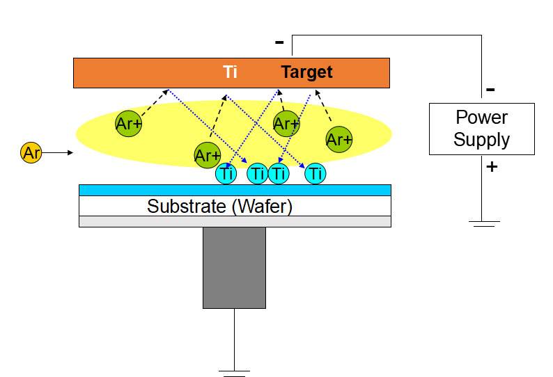
The Physical Vapor Deposition (PVD) process is a meticulous sequence of steps designed to ensure the precise deposition of thin films on substrates. This process begins with the vaporization of the plating material, a critical step that involves heating the material to its boiling point under vacuum conditions. This heating causes the material to transition from a solid or liquid state to a gaseous state, breaking it down into its constituent atoms, molecules, or ions.
Once vaporized, these atoms, molecules, or ions undergo a controlled migration phase. This migration is facilitated by the vacuum environment, which minimizes collisions and allows the particles to travel in a straight path towards the substrate. The vacuum conditions also ensure that the particles maintain their high energy levels, which is essential for effective deposition.
Finally, the particles reach the substrate and begin to deposit, forming a thin film. This deposition process is influenced by several factors, including the energy and angle of incidence of the particles, the surface properties of the substrate, and the vacuum pressure. The result is a uniform and dense film that adheres strongly to the substrate, providing the desired functionalities and properties.
| Step | Description |
|---|---|
| Vaporization | Heating the plating material to its boiling point under vacuum to convert it into a gas. |
| Migration | Controlled movement of atoms/molecules/ions through the vacuum towards the substrate. |
| Deposition | Formation of a thin film on the substrate due to the high-energy particles adhering to its surface. |
Each of these steps is crucial for the successful application of PVD in semiconductor manufacturing, offering a versatile and high-quality method for thin film deposition.
Applications and Advantages
Physical Vapor Deposition (PVD) has found extensive applications across a multitude of industries, primarily due to its environmentally friendly nature and the superior quality of the films it produces. Unlike other deposition techniques that may involve harmful chemicals or high-energy processes, PVD operates under vacuum conditions, ensuring that the deposition process is free from pollutants. This makes it an ideal choice for industries where environmental compliance is a critical factor.
One of the standout features of PVD is the uniformity and density of the films it creates. The process results in films that are highly consistent in thickness and structure, which is crucial for applications requiring precise control over material properties. This uniformity is achieved through the controlled vaporization and deposition of material, which ensures that the film adheres closely to the desired specifications.
Additionally, PVD films exhibit strong bonding with the substrates they are applied to. This robust adhesion is a result of the direct deposition process, where the vaporized material condenses and bonds chemically with the substrate surface. This strong bonding not only enhances the durability of the films but also ensures that they remain intact under various operational conditions, making PVD films suitable for applications that demand long-term stability and reliability.
| Advantage | Description |
|---|---|
| Pollution-Free Nature | Operates under vacuum conditions, ensuring no harmful emissions during process. |
| Uniform and Dense Films | Produces highly consistent films with precise thickness and structure. |
| Strong Bonding with Substrates | Ensures robust adhesion, enhancing durability and long-term stability. |
In summary, the combination of these advantages makes PVD a preferred choice for industries ranging from electronics and optics to aerospace and automotive, where the quality and reliability of thin films are paramount.
Methods of PVD
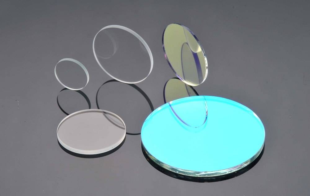
Physical Vapor Deposition (PVD) encompasses several sophisticated techniques designed to deposit thin films with precise functionalities under vacuum conditions. These methods are pivotal in various industrial applications due to their ability to produce high-quality, uniform, and densely bonded films.
The primary PVD methods include:
-
Vacuum Thin Film Coating: This method involves vaporizing a material in a vacuum chamber and allowing the vapor to condense on a substrate. The process ensures minimal contamination and excellent control over film thickness and uniformity.
-
Sputtering PVD: Sputtering involves bombarding a target material with high-energy particles (ions) to dislodge atoms, which then deposit onto a substrate. This method is particularly effective for depositing a wide range of materials, including metals, alloys, and compounds.
-
Ion-Coating: In this technique, ions are accelerated towards a substrate to enhance the adhesion and density of the deposited film. Ion-coating is known for its ability to produce highly adherent and durable coatings, making it ideal for applications requiring robust protection.
Each of these methods offers unique advantages, making them suitable for different applications in semiconductor manufacturing and beyond.
Related Products
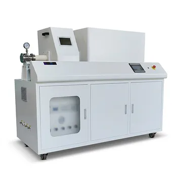
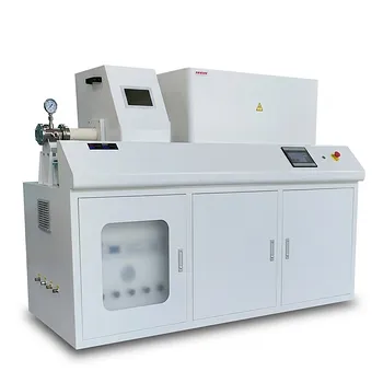
- Inclined Rotary Plasma Enhanced Chemical Vapor Deposition PECVD Equipment Tube Furnace Machine
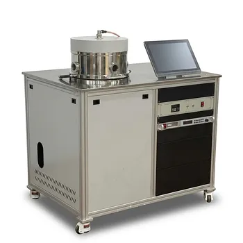
- RF PECVD System Radio Frequency Plasma-Enhanced Chemical Vapor Deposition RF PECVD
- Inclined Rotary Plasma Enhanced Chemical Vapor Deposition PECVD Equipment Tube Furnace Machine
- Chemical Vapor Deposition CVD Equipment System Chamber Slide PECVD Tube Furnace with Liquid Gasifier PECVD Machine
- Electron Beam Evaporation Coating Oxygen-Free Copper Crucible and Evaporation Boat
Related Articles
- A Comprehensive Guide to PECVD Equipment Maintenance
- Plasma Enhanced Chemical Vapor Deposition (PECVD): A Comprehensive Guide
- A Step-by-Step Guide to the PECVD Process
- Understanding PECVD: A Guide to Plasma-Enhanced Chemical Vapor Deposition
- Comparing the Performance of PECVD and HPCVD in Coating Applications
