Articles
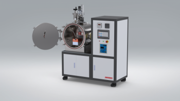
How Vacuum Induction Melting Ensures Unmatched Reliability in Critical Industries
1 year agoVacuum induction melting (VIM) ensures metallurgical purity, durability, and efficiency in aerospace, nuclear, and critical industries. Learn why VIM outperforms traditional methods.
Learn More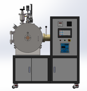
How Vacuum Induction Melting Powers Superior Material Performance in Critical Industries
1 year agoDiscover how Vacuum Induction Melting (VIM) ensures 99.99% pure alloys for aerospace and medical industries, boosting performance and compliance.
Learn More
How Freeze-Drying Cuts Transport Costs by 90% in Critical Logistics
1 year agoFreeze-drying slashes transport costs by 90% in logistics for space, military, and disaster relief by reducing weight and volume. Learn how it works.
Learn More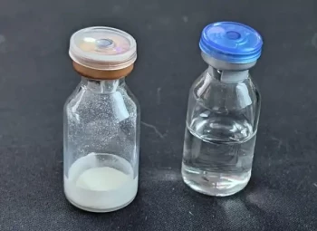
Freeze-Drying Decoded: The Science Behind Preserving Food, Medicine, and Research Materials
1 year agoDiscover how freeze-drying preserves food, medicine, and research materials with unmatched efficiency. Learn the science behind lyophilization and its applications.
Learn More
Why Freeze-Drying is Indispensable for Preserving Sensitive Samples
1 year agoFreeze-drying preserves sensitive samples by sublimation, maintaining molecular integrity and enabling stable, room-temperature storage. Essential for proteins, vaccines, and volatile compounds.
Learn More
How Freeze-Drying Protects Delicate Biological Structures During Water Removal
1 year agoFreeze-drying preserves biological samples by removing water without structural damage, ideal for vaccines, enzymes, and microbial cultures. Learn how it works.
Learn More
How Laboratory Freeze Dryers Outperform Alternatives in Pharma, Food, Biotech & Research
1 year agoDiscover how lab freeze dryers outperform traditional methods in pharma, food, biotech & research—preserving potency, nutrients & integrity.
Learn More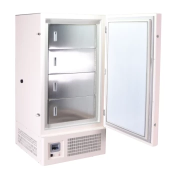
How Cascade Refrigeration Powers Ultra-Low Temperature Freezers Beyond Single-Stage Limits
1 year agoLearn how cascade refrigeration enables ultra-low temperature freezers to reach -80°C and beyond, overcoming single-stage system limitations for critical sample storage.
Learn More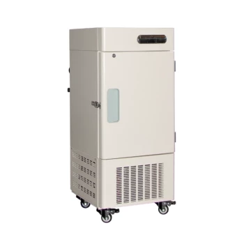
Why Ultra-Low Temps are Non-Negotiable: The Science Behind Preserving Critical Biological Materials
1 year agoDiscover why ultra-low temperature freezers (-86°C) are vital for preserving cells, proteins, and vaccines. Learn the science behind ULT storage best practices.
Learn More
Upright vs. Chest ULT Freezers: How to Choose the Right Configuration for Your Lab
1 year agoCompare upright vs. chest ULT freezers for your lab: temperature stability, workflow efficiency, and cost analysis to protect sensitive samples.
Learn More
How ULT Freezers Prevent Catastrophic Loss of Microbiological Samples
1 year agoULT freezers safeguard microbiological samples with advanced temperature control, contamination prevention, and emergency backup systems to prevent catastrophic loss.
Learn More
Beyond the Spec Sheet: Matching Freeze Dryer Capabilities to Your Application's Critical Needs
1 year agoChoose the right freeze dryer for pharma, food, or biotech. Key specs like cold trap temp, vacuum, and cooling rate impact drying speed and product quality.
Learn More
How ULT Freezers Protect Scientific Discoveries in Genetics and Drug Development
1 year agoULT freezers safeguard genetic and pharmaceutical research by maintaining -80°C storage for DNA, proteins, and cell lines—preventing sample degradation and ensuring research validity.
Learn More
Preserving the Irreplaceable: How ULT Freezers Protect Critical Samples Across Industries
1 year agoULT freezers at -80°C protect biological samples, vaccines, and research materials from degradation, ensuring long-term viability across industries.
Learn More
Polytetrafluoroethylene (PTFE): How low friction coefficient promotes industrial progress
1 year agoExplore the unique advantages of polytetrafluoroethylene (PTFE)'s low coefficient of friction and analyze how it promotes progress and innovation in industrial technology in terms of reducing wear and improving equipment efficiency.
Learn More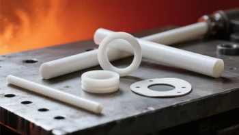
Performance and application of polytetrafluoroethylene (PTFE) in high temperature environment
1 year ago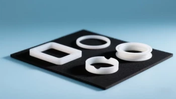
PTFE seals: the invisible guardian of industrial leakage prevention
1 year agoPTFE Seals are used to prevent liquid or gas leakage and are widely used in valves, pumps, and piping systems.
Learn More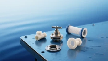
PTFE's high temperature and corrosion resistance: Why it is indispensable in industry
1 year agoThe unique advantages of polytetrafluoroethylene (PTFE) in high temperature and corrosion resistance analyze why it has become an indispensable material in industry, especially in applications in harsh environments.
Learn More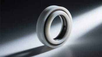
Innovative Application of PTFE in Mechanical Seals
1 year agoPTFE has become one of the core materials in the field of mechanical seals due to its unique chemical stability, low friction coefficient (0.04-0.15), wide temperature range (-268°C to +315°C) and excellent corrosion resistance (pH 0-14).
Learn More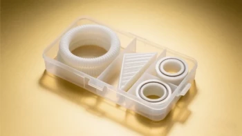
The key role of PTFE in semiconductor manufacturing: from gas pipelines to electrical insulation
1 year agoFrom high-purity gas delivery pipelines to precision electrical insulation components, the multi-faceted application of PTFE in the semiconductor industry chain provides important guarantees for the purity, stability and reliability of the manufacturing process.
Learn More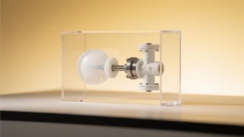
How to use PTFE to improve the working efficiency of pumps and valves
1 year agoPolytetrafluoroethylene (PTFE) has become a key material for improving the efficiency of pumps and valves due to its unique physical and chemical properties.
Learn More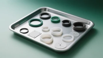
PTFE gasket: an all-around solution for flange sealing
1 year agoPolytetrafluoroethylene (PTFE) gaskets have become an ideal choice in the field of flange sealing due to their unique chemical stability and high temperature resistance.
Learn More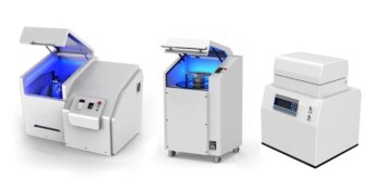
Development and Principles of Frozen Tissue Crushers
1 year agoExplore the history, classification, and principles of frozen tissue crushers, including grinding ball selection and how to choose the right crusher.
Learn More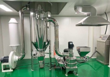
Application of Ultra-Micro Pulverization Technology in the Food Industry
1 year agoExplores the benefits and applications of ultra-micro pulverization technology in enhancing food processing and nutrient absorption.
Learn More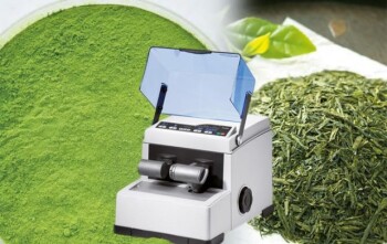
Cryogenic Pulverization Technology and Its Applications
1 year agoExplores the process, advantages, disadvantages, and applications of cryogenic pulverization in various fields.
Learn More
Application of Liquid Nitrogen in Food Freezing
1 year agoExplores the use of liquid nitrogen in food freezing, its advantages, methods, equipment, and safety considerations.
Learn More
Application of Low-Temperature Pulverization Technology in the Spice Industry
1 year agoExplores the benefits of low-temperature pulverization for maintaining spice quality and efficiency.
Learn More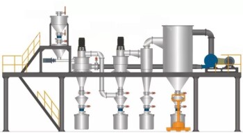
10 Common Dry Ultrafine Crushing Processes
1 year agoOverview of various dry ultrafine crushing methods and their components.
Learn More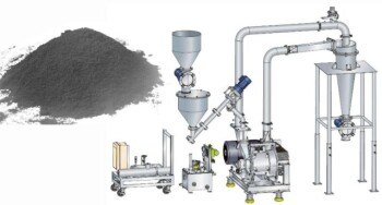
Techniques and Methods of Freeze Pulverization for Powdered Rubber
1 year agoAn overview of various methods for producing powdered rubber through freeze pulverization, including liquid nitrogen and air turbine expander cold methods.
Learn More
Precision Ceramic Materials for Energy Conversion Applications
1 year agoOverview of various ceramic materials used in energy conversion technologies, including heaters, piezoelectric ceramics, and solid oxide fuel cells.
Learn More