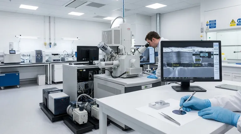
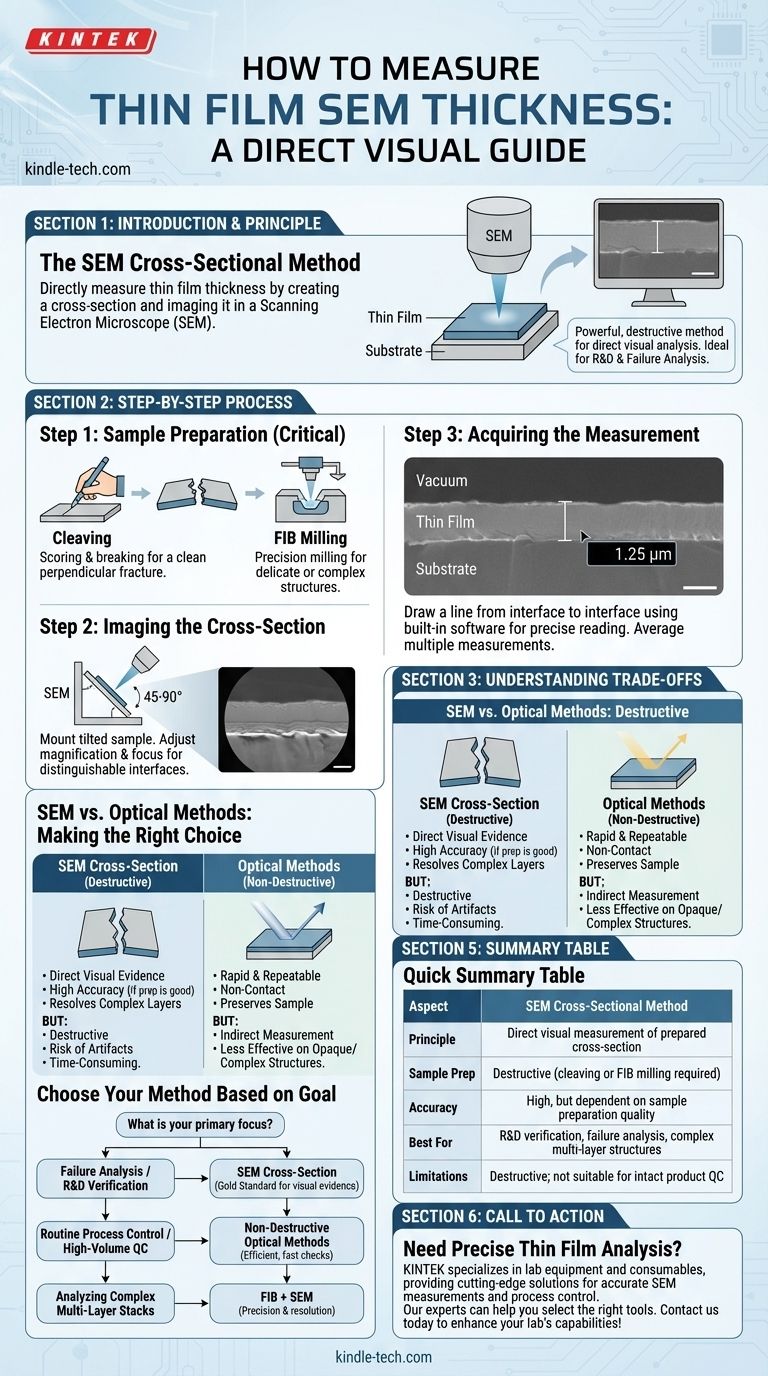
To measure the thickness of a thin film with a Scanning Electron Microscope (SEM), you must first create a cross-section of your sample to expose the film's edge. This cross-section is then imaged in the SEM, and the microscope's built-in software is used to measure the distance directly across the visible film layer. This technique provides a direct, visual confirmation of thickness.
Measuring thin film thickness with an SEM is a powerful but destructive method that offers direct visual analysis. Its accuracy is critically dependent on how well the sample is prepared, making it ideal for verification and failure analysis rather than routine process control.
The SEM Cross-Sectional Method: A Visual Guide
The core principle behind using an SEM for thickness measurement is simple: you have to see the layer to measure it. This requires physically breaking or cutting the sample to reveal a profile view of the film on its substrate.
Step 1: Sample Preparation (The Critical Stage)
The most important step is creating a clean cross-section. A poor cut will lead to an inaccurate measurement.
A common method is to cleave the sample. This involves scoring the back of the substrate (e.g., a silicon wafer) with a diamond scribe and then gently breaking it. The goal is to produce a clean fracture that runs perpendicularly through your thin film.
For more precise or delicate structures, a Focused Ion Beam (FIB) system, often integrated with an SEM, can be used to mill away a small section and create a perfect, smooth cross-sectional face for imaging.
Step 2: Imaging the Cross-Section
The prepared sample is mounted inside the SEM chamber, typically tilted at a high angle (e.g., 45-90 degrees) so the electron beam can scan directly across the exposed edge.
The SEM operator adjusts magnification and focus to get a sharp image where the thin film, the substrate below it, and the vacuum above it are all clearly distinguishable. The contrast between materials in the SEM image makes the layer interfaces visible.
Step 3: Acquiring the Measurement
Using the SEM's integrated software, you can draw a line directly on the image from the substrate-film interface to the film-vacuum interface. The software instantly calibrates this line to the image's magnification and provides a precise thickness reading.
For best results, several measurements should be taken at different points along the cross-section and averaged to account for any slight variations in film uniformity.
Understanding the Trade-offs
While powerful, the SEM cross-section method is not always the right choice. You must understand its inherent compromises compared to other techniques.
The Destructive Nature of Cross-Sectioning
The most significant drawback is that the method is destructive. You must break or cut your sample to perform the measurement. This makes it unsuitable for quality control on a finished product you intend to use or sell.
The Risk of Measurement Artifacts
An imprecise cleave can cause the film to delaminate, smear, or chip, leading to a measurement that does not reflect the true thickness. Furthermore, if the sample is not imaged at a perfect 90-degree angle to the cross-section, projection errors can artificially inflate the measured thickness.
Comparison to Non-Destructive Methods
Techniques like spectrophotometry or ellipsometry are optical, non-contact, and non-destructive. They work by analyzing how light reflects off the film and can measure thickness very quickly over a specific area. These methods are ideal for rapid, repeatable process monitoring where the sample must be preserved. However, they provide an indirect measurement and are less effective on opaque or multi-layered complex structures.
Making the Right Choice for Your Goal
The best measurement technique depends entirely on your objective.
- If your primary focus is failure analysis or R&D verification: The SEM cross-section is the gold standard, as it provides direct visual evidence of the film's structure, interfaces, and potential defects.
- If your primary focus is routine process control or high-volume manufacturing: Non-destructive optical methods like spectrophotometry are far more efficient for quick, repeatable checks that do not damage the sample.
- If your primary focus is analyzing a complex, multi-layer stack: A combination of FIB for precise cross-sectioning and SEM for imaging is the most powerful method for resolving and measuring each individual layer.
Ultimately, choosing the right tool requires understanding whether you need to see the film directly or simply need a fast, repeatable number.
Summary Table:
| Aspect | SEM Cross-Sectional Method |
|---|---|
| Principle | Direct visual measurement of a prepared cross-section |
| Sample Prep | Destructive (cleaving or FIB milling required) |
| Accuracy | High, but dependent on sample preparation quality |
| Best For | R&D verification, failure analysis, complex multi-layer structures |
| Limitations | Destructive; not suitable for intact product QC |
Need precise thin film analysis for your lab? KINTEK specializes in lab equipment and consumables, serving laboratory needs with cutting-edge solutions. Our experts can help you select the right tools for accurate SEM measurements and efficient process control. Contact us today to enhance your lab's capabilities and ensure reliable results!
Visual Guide
Related Products
- Battery Lab Equipment 304 Stainless Steel Strip Foil 20um Thick for Battery Test
- Thin-Layer Spectral Electrolysis Electrochemical Cell
- Laboratory CVD Boron Doped Diamond Materials
- Chemical Vapor Deposition CVD Equipment System Chamber Slide PECVD Tube Furnace with Liquid Gasifier PECVD Machine
- RF PECVD System Radio Frequency Plasma-Enhanced Chemical Vapor Deposition RF PECVD
People Also Ask
- What are the primary considerations for selecting Stainless Steel 304 as an electrode material? Ensure Safe Water Care
- What are pure silicon sputtering targets? Precision Source for High-Performance Thin Films
- What is the process of cathode sputtering? A Step-by-Step Guide to Thin Film Deposition
- Can silicon be sputtered? A Guide to RF & DC Methods for Thin Film Deposition
- What is diode sputtering? A Guide to the Fundamental Thin-Film Deposition Process